Compilation of notes for Fundamentals of Computer Systems class for Spring 2023.
- Problem Solving Tips
- Administrative Stuff
- Lecture 0
- Lecture 1
- Lecture 2
- Lecture 3
- Lecture 4
- Lecture 5
- Latch Intuition
- SR Latch
- SR Latch with Control
- D Latch with control
- Flip Flops
- Registers
- MIPS Programming
- Architectures
Problem Solving Tips
- Break down problems into manageable sub-problems
- If you get stuck, take a break, then slowly and methodically think through the sticking point (ie. break it down more. Make sure you are reading the problem correctly)
- Write in your own words what you need to do
- Remember that everything happens in parallel, and you only keep the results that you want
Administrative Stuff
Exams
- Midterm: On March 8th, 6-9 pm (tentative)
- Check for conflicts
- End-of-term exam: Either April 27, evening (6-9 pm) or May 5 in the evening
- Fill in exam conflicts (by 1/24)
- Acceptable excuses: conflicting classes and religious conflicts
- Fill in P-credit office hours (By 1/21)
- Go to web form
- The top row indicates the start time of the office hours (e.g. 12 means 12-1. 12:30 means 12:30-1)
- Need at least 10 hours selected
- Email for help: 3827-staff[at]googlegroups.com
- Include 3827 in subject header. Otherwise, it will get overlooked
- Use EdStem for class updates instead of Courseworks, as well as to ask questions b/c it will be faster than email
Grades
- P Credit has a score between 0 to .3
- P = 0 you never attend
- P = .3 you attend every P-cred and actively participate
- The final grade is G = 100P+(1-P)(10H+max(30M+60F,45M+45*F))
- H is the percent correct on the HW
- M is the percent correct on the midterm
- F is the percent correct on the final
Lecture 0
- Work on HW0 (Not graded)
- Why should I care about this course?
- Shows how computers run “under the hood”
- Learn “parallel thinking”
- Humans think sequentially
- Circuits run multiple “threads” at once
- Useful to understand these ideas in many domains
- Systems
- Programming Languages (Compilers and Interpreters)
- Quantum Computing
- ML/AI
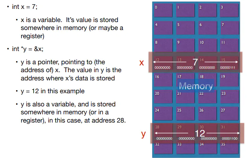
Lecture 1
CPU Models
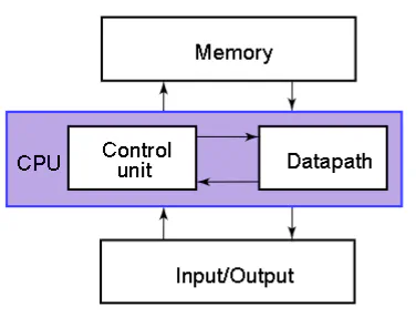
- CPU: “brain” of the computer
- Control Unit: D oes calculations on data in datapath
- Memory: Stores data (for later use)
- I/O: Interface to the outside (disk, network, monitor, keyboard, mouse, etc.)
- Simpler model of CPU:
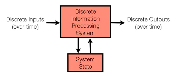
- Discrete inputs (over time)
- Discrete Information Processing System
- communicates with System state and output something based on input
- System State
- Remembers previous information
Addition in different bases
- humans: 10 digits: {0,1,2,3,4,5,6,7,8,9}
- $(4537.8)_{10} = 4*10^{3}+5*10^{2}+3*10{1}+7*10^{0}+8*10^{-1}$
- Shifting everything to the left is multiplication by 10
- computers: 2 digits: {0,1}
- $(1011.1)_{2} = 1*2^{3}+0*2^{2}+1*2^{1}+1*2^{0}+1*2^{-1} = 11.5$
- Shifting everything to the left multiplies by 2
- Hex: 16 digits {0,1,2,3,4,5,6,7,8,9,A,B,C,D,E,F}
- Hex numbers specified as 0x26BA
- $0x26BA = 2*16^{3}+6*16^{2}+11*16^{1}+10*16^{0} = (9914)_{10}$
- We use hex since it is more human readable and is easy to convert to and from binary
- a base-2 4 digit can be multiplied by 16 by shifting 4 to the left ($1100 \rightarrow 1100\ 0000$)
- a base-16 1 digit can be multiplied by 16 by shifting 1 to the left ($0xD \rightarrow 0xD0$)
- To convert binary to hex, break hex into groups of 4 and convert each group to corresponding binary number
- $0010\ 1011 \rightarrow 0x2B$
- For hex to binary, just convert each hex digit to the corresponding group in binary
- $0x2B \rightarrow 0010\ 1011$
Definitions
- True = 1, False = 0
- Everything eventually converted to either 1 or 0
- Numbers: 19 base 10 = 10011 base 2
- Letters: each character is assigned to a 8 bit number
- Bits:
- a single binary digit (0 or 1)
- The leftmost bit is the highest order bit
- The rightmost bit is the lowest order bit
- Byte:
- A group of 8 bits. e.g. (10110010)
- Word:
- a grouping of bits
- computer-architecture dependent
- The number of bits that the computer architecture can process at once
- 64-bit word architectures expect data in 64-bit groupings
- The number of bits used by an architecture is called the word size
- 64-bit word architectures expect data in 64-bit groupings
- Common notation for k-bit value: $b_{k-1}b_{k-2}…b_{1}b_{0}$
- a grouping of bits
Modular Arithmetic
- Def: X mod Y = remainder (X/Y)
- remainder constrained between 0 and Y-1
- Alternative definition: remainder constrained between $-\frac{Y}{2}$ and $\frac{Y}{2}-1$
- 100 mod 9 = 1
- -10 mod 3 = -1 mod 3 = 2 mod 3
- X mod Y = Z mod Y iff
- $X = Z+KY$ for some integer K
- X mod Y = Z mod Y iff
Integer format with word size restriction
- For a given number of digits, how many possible values can you represent?
- $b^{d}$, where b is the base and d is the number of digits
- For 2 bit word size: {00, 01, 10, 11}
- As humans, we can assign whatever value to a distinct bit-sequence:
- 2 bit word size: {00: .234, 01:i, 10: 234, 11: asdf}
- Nonsensical , but allowed
- 2 bit word size: {00: .234, 01:i, 10: 234, 11: asdf}
- $b^{d}$, where b is the base and d is the number of digits
Unsigned binary numbers
- Positive integers of a fixed wordsize
- e.g. 1111 = 15 for a 4-bit word
Binary Addition Algorithm (BAA)
- 1+1 = 0 with a carry of 1
- eg. wordsize = 5, add 11110 and 10101 (30+21)
- 11110+10101 = 10011 if restricted to 5 bits
- Called overflow: when a result can’t fit within the wordsize constraint
- The correct answer needs 6 bits (110011)
- 11110+10101 = 10011 if restricted to 5 bits
- The answer may not be correct because of overflow, but it is correct up to mod $b^{d}$
Negative numbers
Signed Magnitude Representation
- Let the highest order bit denote the sign of the number (0 is positive and 1 is negative)
- e.g. 0011 = 3
- e.g. 1011 = -3
- e.g. 1000 = 0000 = 0
- To negate, simply flip the highest order bit
1’s Complement
- Again, highest order bit indicates sign (0 is positive and 1 is negative)
- To negate a value, flip all the bits
- 0010 = 2
- 1101 = -2
- e.g. wordsize of 8, value is 11101001. 1’s Complement rep
- We know its negative (1 in highest order)
- Negate all the bits and read off positive value, then slap on negative sign
- Using this, 11101001 = -20
- 000000 = 111111 are both 0 in 1’s complement
Problems with Signed Magnitude and 1’s Complement
- 0101+1101 = 0010 (after dropping carry of 1)
- Unsigned binary: 5+8 = 2 (correct mod 16)
- Signed magnitude: 5+ (-5) = 0 (not 2, even up to mod 16)
- 1’s complement: 5+(-2) = 3 (not 2, even up to mod 16)
- TL;DR Binary Addition Algorithm doesn’t work
2’s complement
- highest order bit is still sign
- To negate a number, flip all the bits (like 1’s complement) then add 1 in binary (eg a 4 bit word size, you add 0001)
- 0010 = 2 so 1101+0001 = 1110 = -2
- 1101 = -3 so 0010+0001 = 0011 = 3 (works for negative)
- 0 is unique in 2’s complement (0000 = 1111+0001 = 0000)
- “100000” maps to itself in 2’s complement (largest negative number of the word size)
- 2’s complement always work with BAA (meaning that with any overflow, the result is off by mod $2^{wordsize}$)
Intuition behind 2’s complement
- Let X be some word of size k
- Negate all the bits of X and call it Y
- e.g. X = 100101, so Y = 011010
- $X+Y$ using BAA always equals a a word of size k whose entries are entirely 1s
- $X+Y$ = 111111
- Adding the the decimal number 1 to $X+Y$ (ie 000001) causes overflow which yields a word of only zeros.
- So we can think of the operation of flipping all the bits and adding decimal 1 to a string as the negation of X
Lecture 2
- The range of unsigned integers is 0 to $2^{k}-1$
- The range of signed integers is $-2k^{k-1}$ to $2k^{k-1}$
- A string if bits is useless unless you know what representation they represent (unsigned, signed ,ASCII, etc.)
- Representation: How you interpret the bits
- Operations: do something to the bits (independent of representation)
Why 2’s complement?
Easy subtraction
- Say that we want to find 001110-010101 in signed magnitude representation (14-21). It the same procedure as in base 10, but in base 2 (including carries)
- Instead, make the representation the 2’s complement
- Negate 21, then apply BAA. You get the correct answer: 001110-010101=001110+101011=111001 (14-21=7)
Detecting Overflow
- For 2’s complement:
- Look at the final 2 carries from the BAA algorithm. If the carries are different, you have overflow
- $00$ case: $5+1=6\rightarrow 0101+0001=0110=6$
- $11$ case: $-5-3=-8\rightarrow 1011+1101=1000=-8$
- $10$ case (overflow): $-2+-7=-9\rightarrow 1110+1001=0111=7$
- $01$ case (overflow): $7+7=14\rightarrow 0111+0111=1110=-6$
- Look at the final 2 carries from the BAA algorithm. If the carries are different, you have overflow
- Overflow just means that the result can’t be represented with the word size. It does not mean that the result is too big
Floating Points
- Scientific notation:
- -7.776E3. The number to the left of the E is called the mantissa. The number to the right is the exponent
- In binary: $-1.10\times2^{01111}= -1.5*2^{7}$
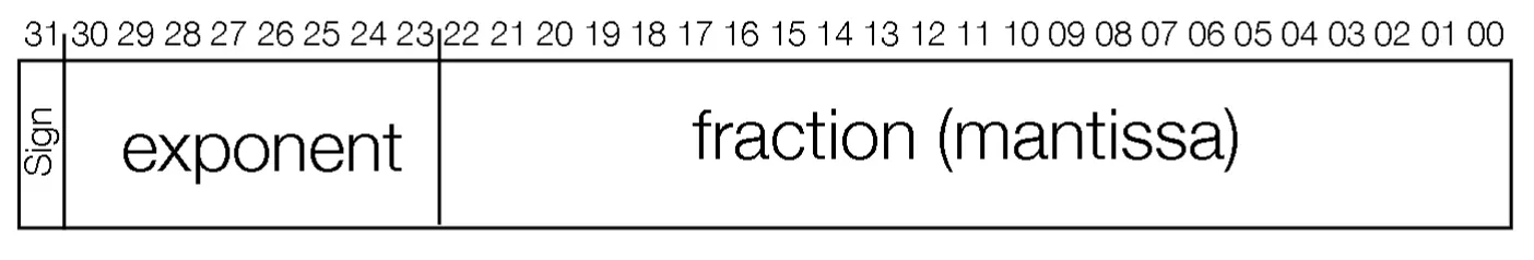
IEEE standard for a 32 bit word
- highest order bit (31th) is the sign
- 0 is positive, 1 is negative
- exponent is bit 30 to 23
- represent the value as an unsigned binary, then subtract 127 (the bias)
- Fraction (the rest of the bits)
- represents 1.XXXXXX. The “1.” is implicit for all floating point numbers, including zero. The mantissa represent the numbers after the decimal
- represents 1.XXXXXX. The “1.” is implicit for all floating point numbers, including zero. The mantissa represent the numbers after the decimal
- To approximate zero, you set all the bits to zero, which corresponds to $1.0*2^{-127}$, which is effectively zero
Doubles
- A double uses two 32-bit words
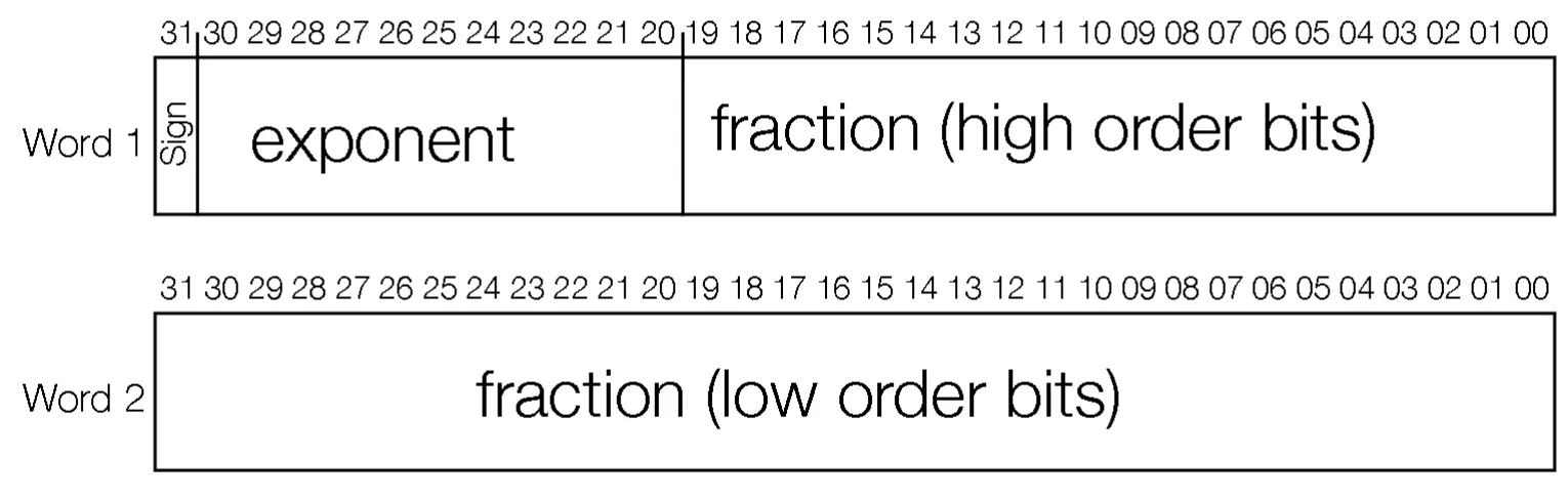
- There is one sign bit, 11 exponent bits, and 52 fraction bits
- The first word has the sign bit, the exponent bits and the rest are the higher order bits of the fraction
- The second word is the rest of the fraction
- The bias is 1023
Underflow
- Say that we have a number X = 1E-83. Squaring X, we get Y = 1E-166. This cannot be represented as a float. This is referred to as underflow, which is a subcategory of overflow
Boolean Algebra
- Either 0 or 1 (False or True)
- Can represent as a variable (X,Y,A,B)
- Complement of X is denoted as $\bar{X}$. This is just flipping a bit
- Literal a boolean variable or its complement
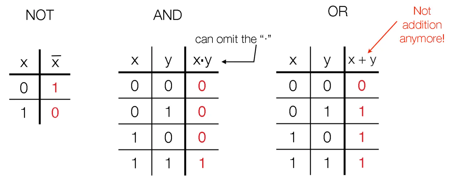
- $\cdot$ represents AND (can be omitted)
- + represents OR
- Left to right precedence. parentheses give priority to operations
- You daisy chain operations on multiple values by constructing a truth table where each column represents an unsigned integer
- Expressions is a set of literals (possibly with repeats) combined with logic operations
- Equations expression1=expression2
- Functions: Takes in some literals and outputs an expression
Boolean Algebra Identities
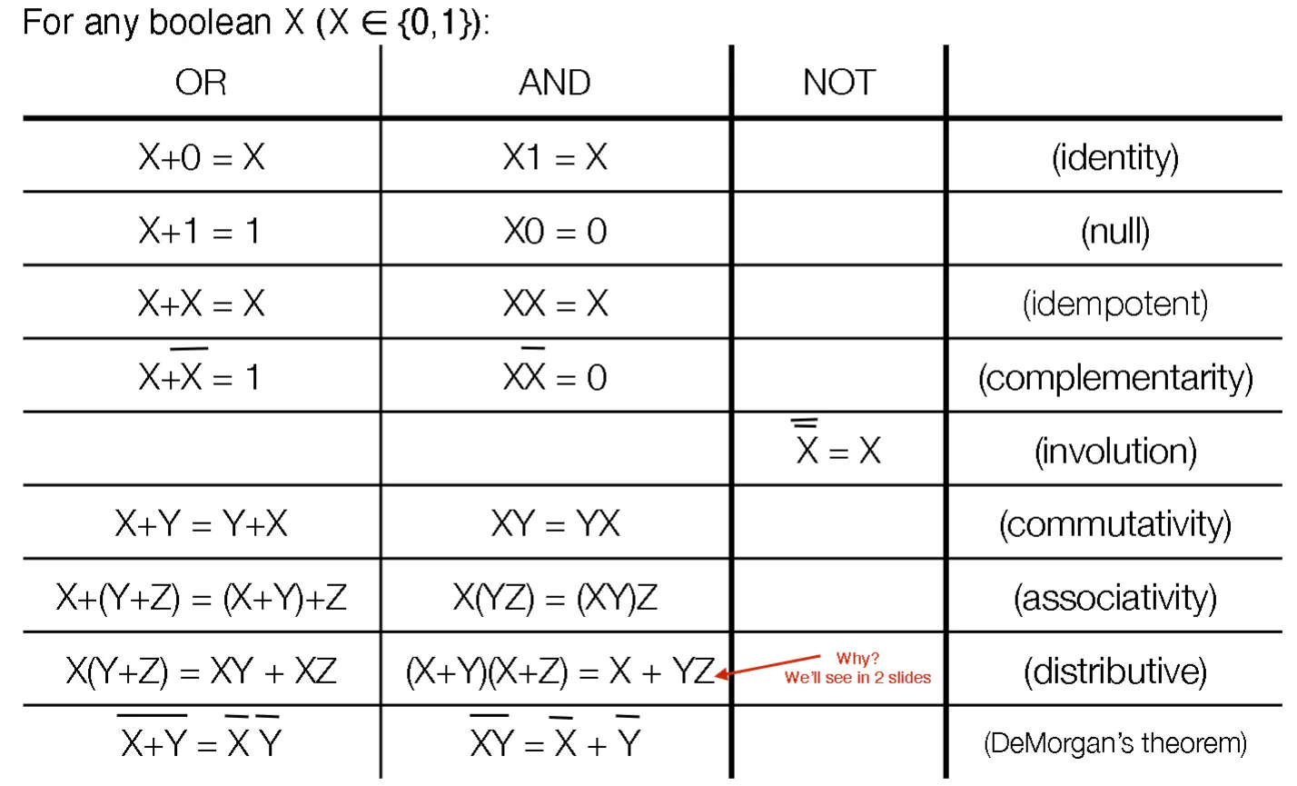
- $X+XY=X$
- $X(X+Y)=X$
Distributive Law Proof
- $(X+Y)(X+Z) = XX+XZ+YX+YZ$
- Apply $XX=X$, $X+XZ = X$, $X+YX=X$ sequentially to show final result
DeMorgan’s Theorem
- Split the big bar at the operator
- Chance AND to OR and OR to AND
- Flip-flop literal 0 and 1 to each other
- Replace function F with the complement $\bar{F}$ and vice versa
Consensus Theorem
- $XY+\bar{XZ}+YZ=XY+\bar{X}Z$
- If $YZ = 0$, then trivially you can drop $YZ$
- If $YZ=1$
- both $Y$ and $Z$ are 1. $XY+\bar{X}Z+1 = 1$, so LHS is 1
- Either $X$ or $\bar{X}$. Since $Y=Z=1$, either $XY$ or $\bar{X}Z$ is 1, so RHS is 1
circuit Representation of Boolean Algebra
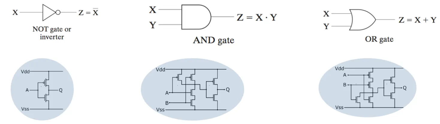
- The depth of a circuit refers to how the maximum layers are between the input and output
- If you want to have multiple inputs, put more lines as the input on the left
- a k-input gate has a depth of $log_{2}(k)$
Coverting Circuits to Booleans
- Start from the RHS and move left
- As you pass each gate, write down the number of inputs in their own section
- Repeat until you get to your inputs
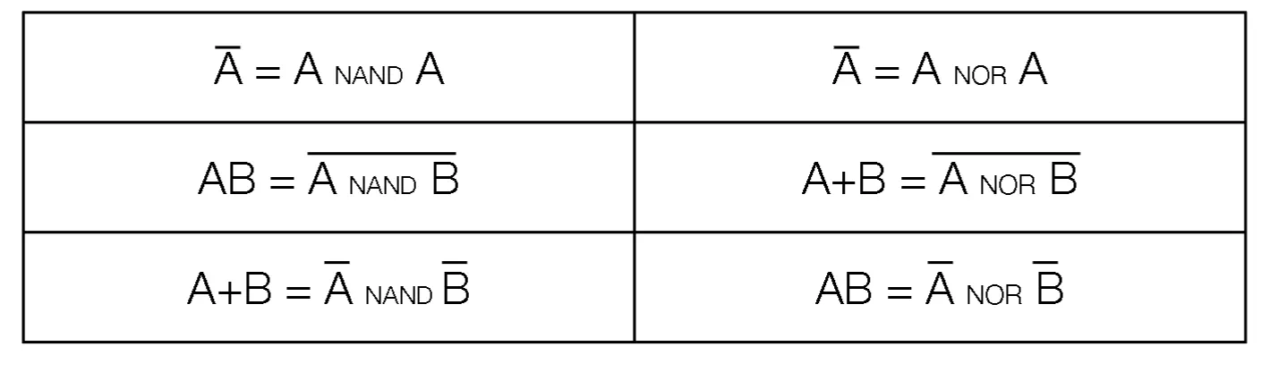
NAND and NOR
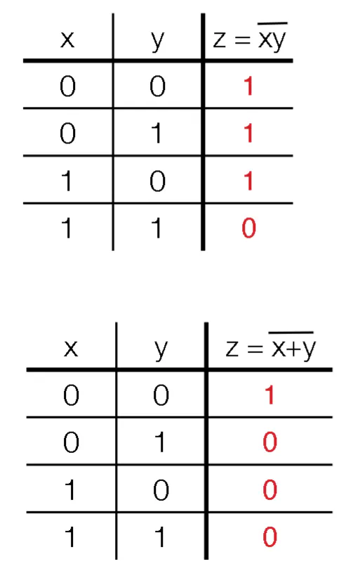
- You invert the output of AND and OR respectively
- These are universal gates
XOR
- XOR is denoted as $\otimes$ (either the first or the second is true, but not both)
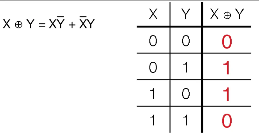
- Used for parity control (how many of the inputs are true)
- $Y\otimes 0 = Y$
- $Y\otimes 1 = \bar{Y}$
- $X_{1}\otimes X_{2}\otimes…X_{k}=1$ when an odd number of $X_{i}=1$
- Used for parity control (how many of the inputs are true)
Duals
- All booleans expressions have duals. TO construct the dual:
- Swap the ANDs and ORs, swap the literals 0 and 1 for each and rearrange the parentheses as needed
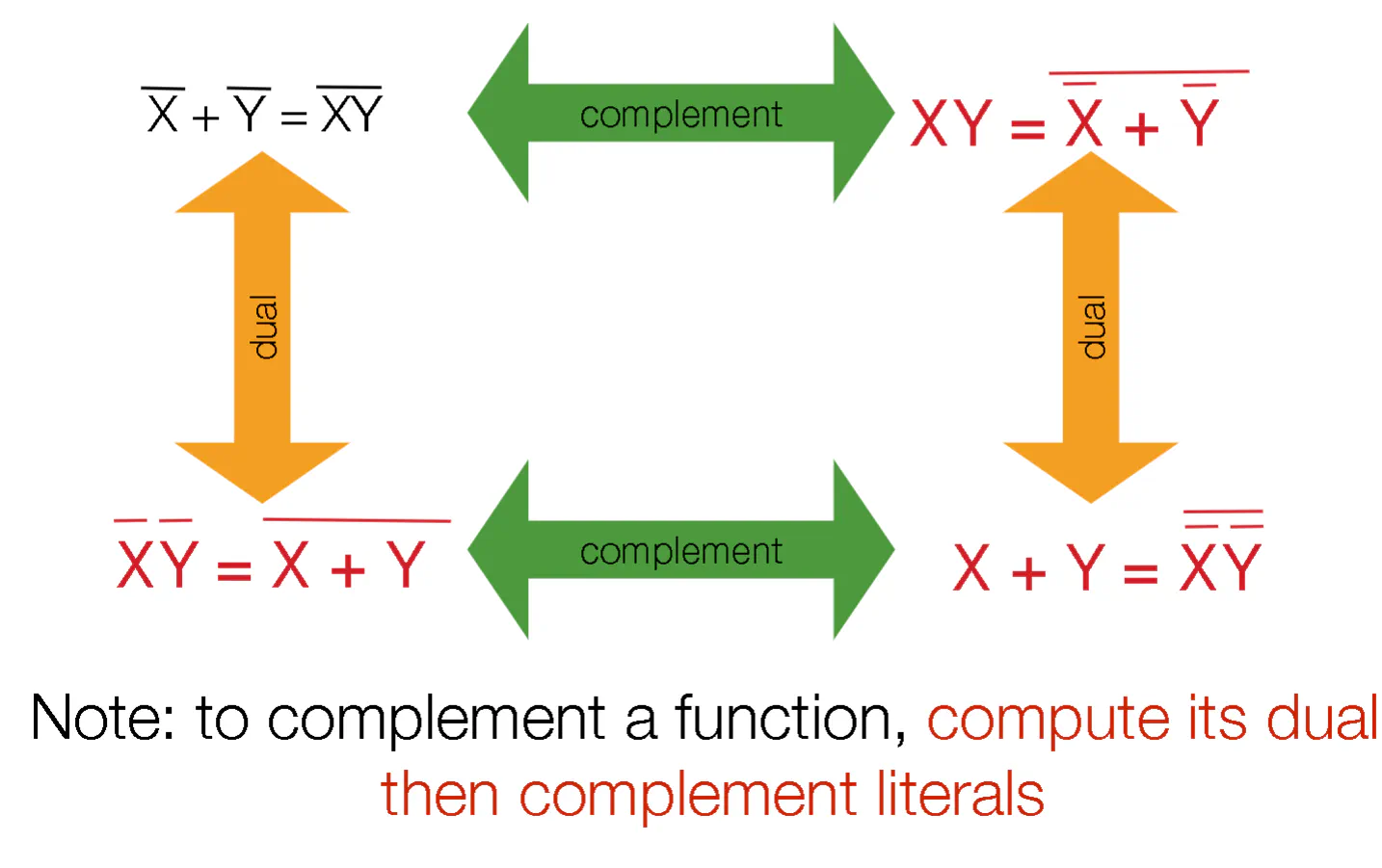
- Swap the ANDs and ORs, swap the literals 0 and 1 for each and rearrange the parentheses as needed
- You can take the complement of a function by taking the dual, then negating all the literals
Lecture 3
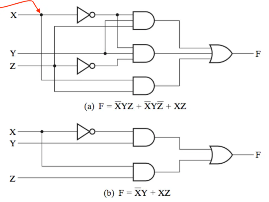
Sum of Products (SoP)
- Any function can be represented as a product of sums (ie. ORing ANDS together)
- Do all the ANDs before the ORs
- To calculate, expand out all the terms, then remove duplicates
- G = X(Y+Z)(X+Y+Z) = XY+XZ
Product of Sums (PoS)
- Any function can be represented as a sum of products (ie. ANDing many ORs together)
- Do all the ORs before the ANDs
Convert SoP to PoS
- onvert function $F$ to SoP. Take the compliment of SoP by taking the dual and then complementing the literals. This is PoS
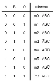
Minterms
- Minterm is a product term in which all variable appear exactly once (either complemented or uncomplemented)
- You can refer to each minterm by the unsigned int that they represent (mX)
- A function can be described as a sum of its minterms
- You can evauluate when the function is true by looking at the minterms
- You can marginalize on a literal by including the minterms that include literal and its complement
- Minterm expansion is not a simplified form
Maxterms
- The dual of minterms (ie a sum in which all variables appear exactly once, either complemented or uncomplemented)
- Denoted as MX
- The product expansion of a function in terms of maxterms
- Whenever the function evaluates to zero, these inputs correspond to a particular maxterm in the expansion
Karnaugh Map
- Say that you have $F = X+\bar{X}Y$. How do you simplify this?
- Replace $X = X+XY$ and turn the crank to get $F=X+Y$
- Not immediately obvious. Need an automatic tool to help
- Not the simplest form, but good enough
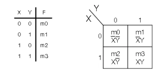
- Expand the truth table into a 2D grid indexed Y horizontally and X vertically (origin from the top-left and moves right and down)
- Each value of the input literal tells you where on the Karnaugh Map
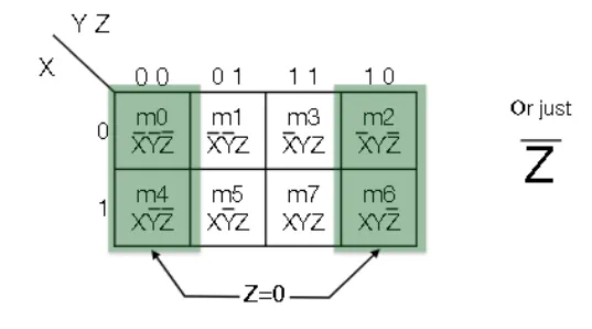
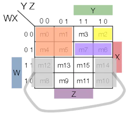
- Let the vertical axis be X, and the horizontal be YZ
- Gray encoding: order values of YZ such that only one bit changes at a time
- Y goes on top, Z goes on bottom
- Let the vertical axis be X, and the horizontal be YZ
- Minterm product terms correspond to a $2^{i} \times 2^{j}$ rectangle (including wraparounds)
- To find the simplest form you can derive from the k-map, you draw the largest rectangles you can (incluing wraparounds) and then relate these rectangles to products
K-map Notation
- Implicant: a product term comprised of minterms for which the function F evaluates to 1 (ie. a box whose dimensions are powers of 2)
- Prime Implicant: there exists no other implicant that can contain this implicant
- Essential Prime Implicant: this implicant covers at least one minterm that is not covered by any other prime implicant
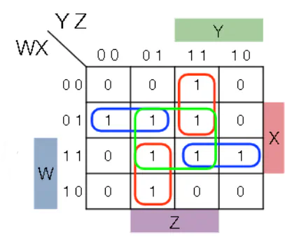
Summary of Simplification with k-maps
- Identify all the prime and essential prime implicants
- Include all the essential PIs
- If any 1-valued minterms are uncovered by EPIs, choose PIs that are “big” and do a good job covering
- Heuristic: Choose the PIs that minimize overlap with one another and with EPIs
2-bit multiplier
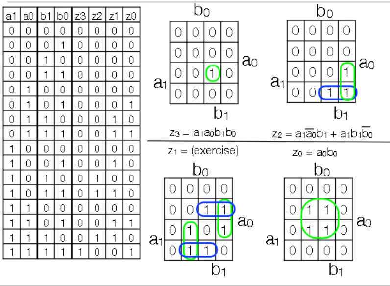
- You have 2 2 bit numbers. You need 4 bits to represent the largest product
- Each bit in the output can be written as a k-map, which can be simplified to write what inputs correspond to this particular output bit getting turned on
Don’t Care Conditions
- These are circumstances where the output doesn’t matter
- Going to the 2-bit multiplier, say that you know that some set of inputs will never occur. Hence you can ignore the output of those inputs when building a circuit
- Denote X as the outputs where you don’t care about the output
- In the k-map, replace the don’t care conditions with X. You can optionally cover X’s with EPI’s (ie. you can include X’s in larger boxes to simplify circuitry)
Drawing Circuits
- Denote a circuit as a blob so you don’t have to redraw a circuit over and over again
- When an input changes, it takes time for the output to get updated
Lecture 4
Standard Circuits
- NB: Think about circuits as having constant input
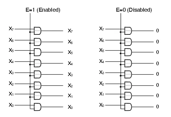
Enabler
- Takes in data D (k bits in parallel), as well as an enable/disable trigger E. There is a single output of k bits
- If E=1, the output equals the input
- If E=0, output equals k 0’s
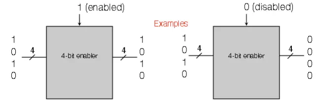
- Implement enabler with k AND gates. Each input has it’s own AND gate, and the other pin is the Enable input
Decoder Circuit
- Takes in a k-bit input and $2^{k}$ 1-bit outputs
- The selector indicates as an unsigned binary which output = 1. All other outputs are zero
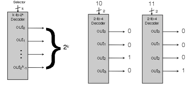
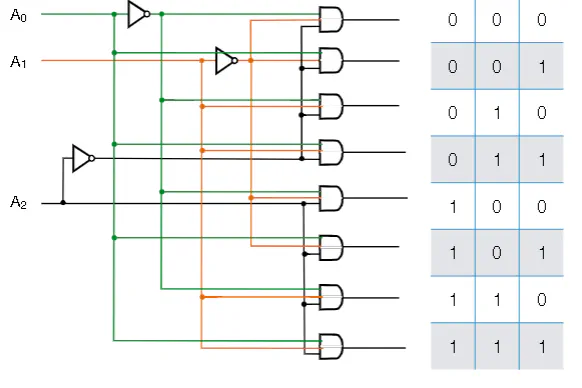
- Write truth table out. Each row is a minterm. Recall that each minterm evaluates for 1 for a unique combination of literals.
- You can write decoders with a combination of NOTs and ANDs
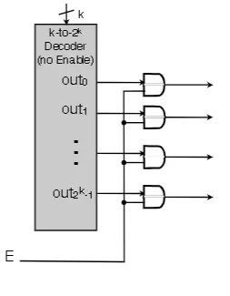
Decoder With Enable
- Slap the two previous circuits together
- Push the output of the decoder through k AND gates where every AND gate has a input connected to the enable pin
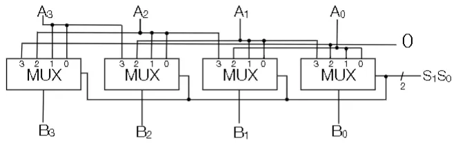
MUX (Multiplexer)
- Takes $2^{k}$ 1-bit data values as input. Has a k-bit selector that indicates in unsigned binary which data bit is output
- You push all the data values in as input simultaneously, and only the one you select is the output. All other inputs are dropped
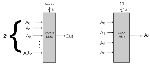
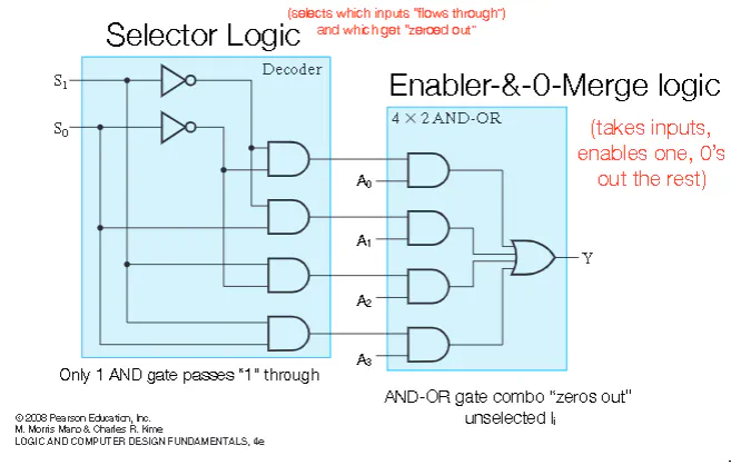
- You have a selector part that chooses which input to select
- You pass all this data to an enabler, whose output gets passed to an OR gate
Representing Functions with Decoders and MUXes
- Use a Decoder and OR together the minterms that evaluate to 1 of your function
- Use a Multiplexer where you feed in the output of your function. The input to the multiplexer is the values that your literals you take. The output is then your function
MUX trick
- Look at your truth table in pairs of rows. You can select on A and B as the selector input. You pass the C input as one of the the $2^{k}$ 1-bit inputs and it’s complement
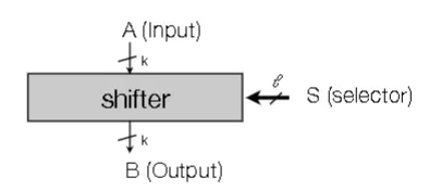
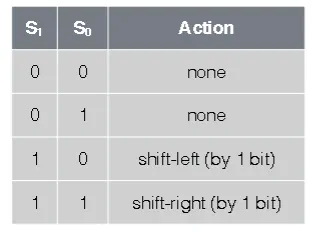
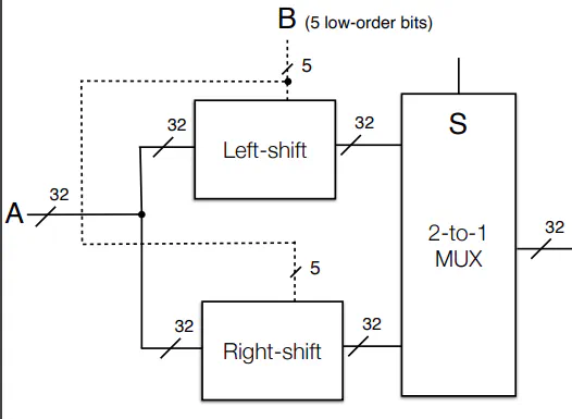
Shifter Circuit
- k-bit data value enter as input
- l-bit selector in unsigned binary tells how many bits to shift
- k-bit output where bits are shifted by l-bits (can wraparound or drop out)
Barrel Shift left w/ Wraparound
- Say you want to shift over by 2 with wrap around
- You use MUXes. Each output bit of the MUX goes to the output of the Shifter. All the MUXes have the same shift bit as their selector
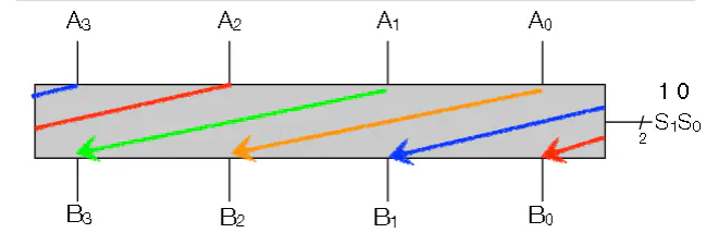
L-R Shift Circuit with Rollout
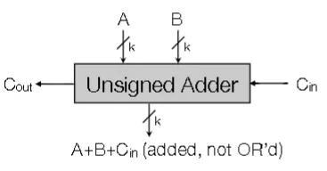
Unsigned Adder Circuit
- Two k-bit data values (A,B) and 1 bit carry in bit $C_{in}$
- output is k-bit of $A+B+C_{in}$ and a carry out bit $_{out}$
Half-Adder
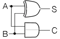
- Takes two inputs A and B and returns a Sum and a carry
- The sum is computed via XOR and the carry is computed by AND
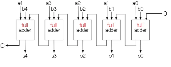
Full-Adder
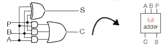
- Takes as input 2 digits (A&B) and previous carry (P)
- Can daisy chain full adders together
- Each subsequent adder needs to wait until the previous adder to finish
Signed Adder/Subtractor (2’s-C)
Ripple Carry Adder
- Two k-bit data values and 1 bit S (0 for add, 1 for subtract)
- Output is k-bit $A+B$ when S is 0 and $A-B$ when S is 1
- You also have an overflow bit
- You also have an overflow bit
- To calculate A-B, first flip B by XORing with 1 prior to sending the output of the XORs to a full adder with an initial carry of 1
- Overflow can be calculated by XORing the highest order bits of the adder
Optimizing Ripple Carry (Carry Lookahead)
- We try to parallelize the carry operations
- When do we get carries
- If the ith bit of A and B are the same (11 or 00), then you are guaranteed to either have a carry or not have a carry respectively
- if the bits are different, what happens?
- There is a carry iff the previous column has a carry
- $C_{i+1} = A_{i}B_{i}+(A_{i}\otimes B_{i})A_{i-1}B_{i-1}$
- This can be recursively expanded to the lowest order bit
Merge with known 0’s
- Suppose we have m input signals
- We know all of them except one is zero. The remaining bit could be zero or one. You also don’t know which one is the unknown bit
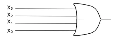
- Implement with an OR gate
Code Converter
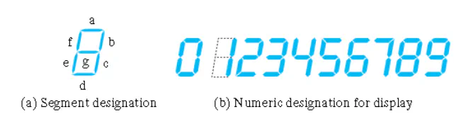
- Say that you want to build a circuit to light up a LED number. Denote each segment of the LED with a letter
- Take in as input 4 variables WXYZ and output which segments to light up
- Look at each column of the truth table, build a k-map from the column and then build a circuit
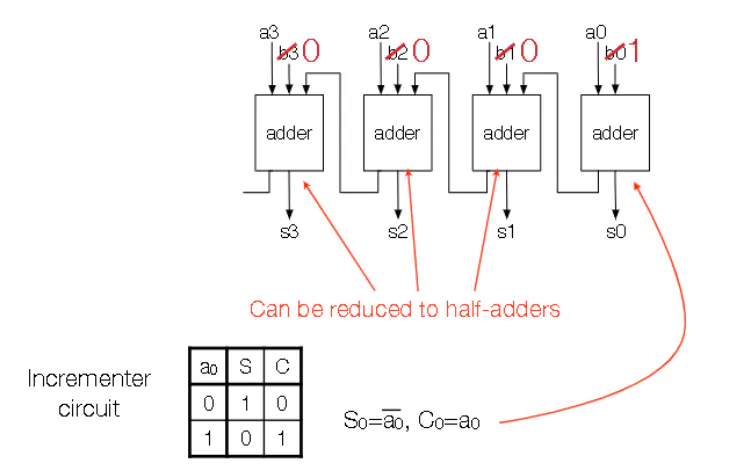
Contraction
- Say that you have a circuit. Now you know that some inputs are fixed. YOu can simplify the circuit
Example 1
- For an incrementor (add one to current value), you can replace full adder with half adders and be careful with the lowest order bit
Lecture 5
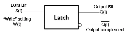
Latch Intuition
- You a data bit X(t), a write bit W(t) and outputs of Q and complement of Q
- If w is 1, then the Q follows X
- If w equals 0, then Q maintains its current output, regardless of the input
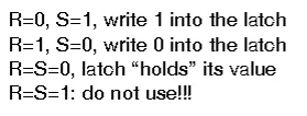
SR Latch
- We have a reset pin (R), a set pin (S), and output and inverted outputs (Q and $\bar{Q}$)
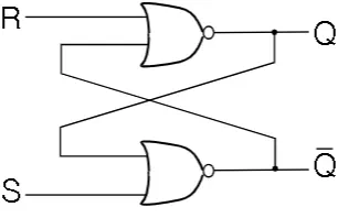
- implemented with NOR gates
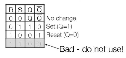
- implemented with NOR gates
- R = 1 and S =1 produces garbage
- You can also construct a $\bar{S}\bar{R}$ Latch with NAND gates, where S=0 and R=0 is garbage instead
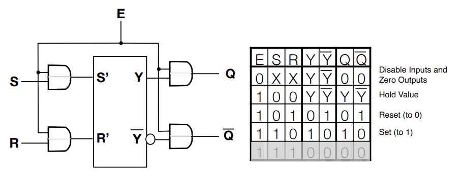
SR Latch with Control
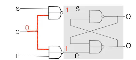
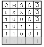
- We have S,R, and C being fed into NAND Gates, whose outputs get feed into $\bar{S}\bar{R}$ latch.
- C controls wheather the latch is enabled or not. If the latch is not enabled, it defaults to holding its current value
D Latch with control
- You have D and C being feed int NAND gates, where you invert one of the C inputs. The results are feed into an $\bar{S}\bar{R}$ latch. Implementation of intuitive idea of latch
Latches Can’t be Clocked
- What this means is that you can get race conditions where a slow function can’t keep up with faster functions
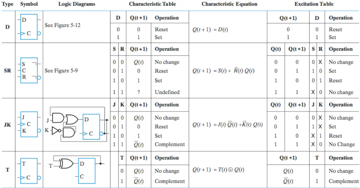
Flip Flops
- You have 2 SR Latches with Controls.
- The control pin of the first is hooked up to a clock and the control pin of the second is hooked up to the negation of the clock
- The outputs of the first latch are hooked up to the second latch
- This setup disallows inputs until the second flip-flop is on
- A full clock cycle is one iteration of the clock going down then up
- Flip-flop releases new values whenever the clock goes from 1 to 0. Alteratively, the first latch is updated when the clock is 1 and the second latch is updated when the clock is 0
- This means that the output of the ith cycle is updated based on the input at the (i-1)th cycle
- You can use other latches (D for instance)
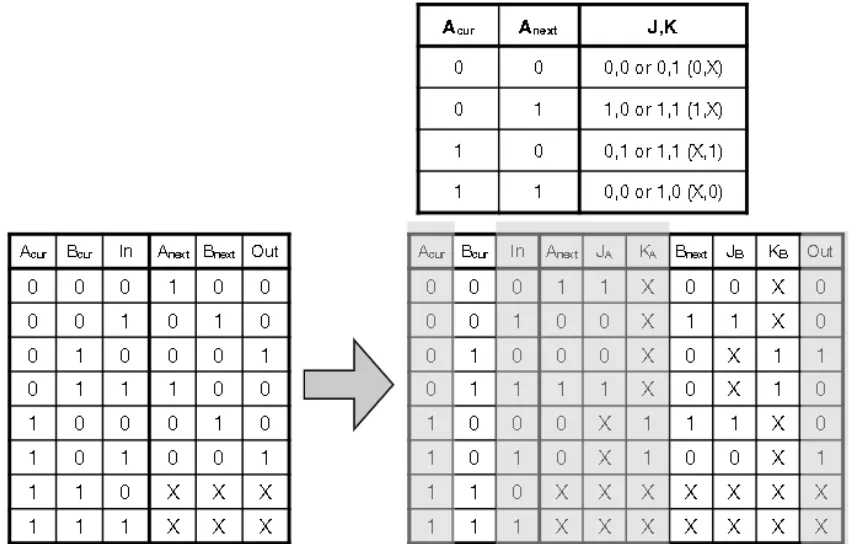
JK Flip Flop (JKFF)
- J =1, K=0
- Regardless of $Q(t)$ value, J=1 and K-0 sets the JKFF to $Q(t+1)=1$
- J=0, K=1
- Regardless of $Q(t)$ value, J=0, K=1 resets JKFF to $Q(t+1)=0$
- J=0, K=0
- THis keeps the current output
- J=1, K =1
- This compliments the current output
Flip Flop Table
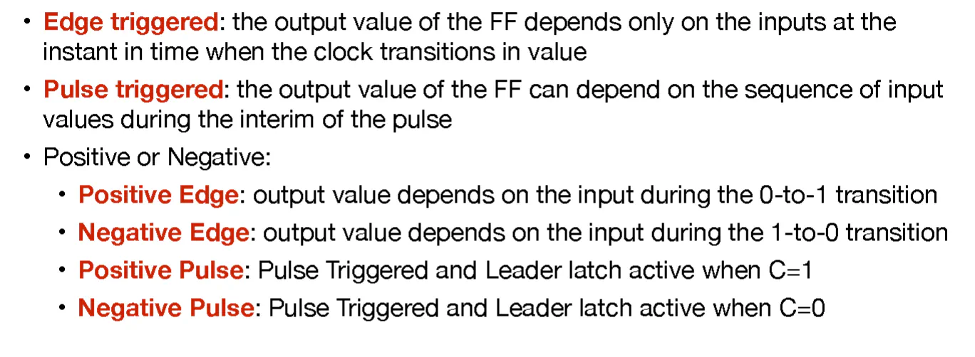
Trigger Types
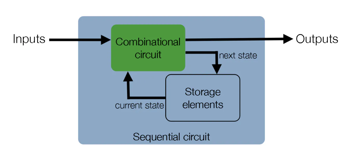
Sequential Circuit
State Machines
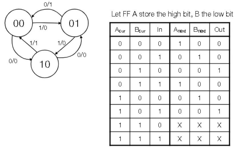
- States are labelled as circles with labels
- Transitions from one state to another are labelled with unidirectional arrows
- Each arrow also have a label of the form $X/Y$ where X is the input and Y is the output
- Arrows can point to any state in the diagram, including the current state
- A state machine can be converted to a sequential circuit
- Enumerate all possible current states
- For each state, figure out where the state machine goes for a given input and write the final state and the output
- Repeat for all possible combinations
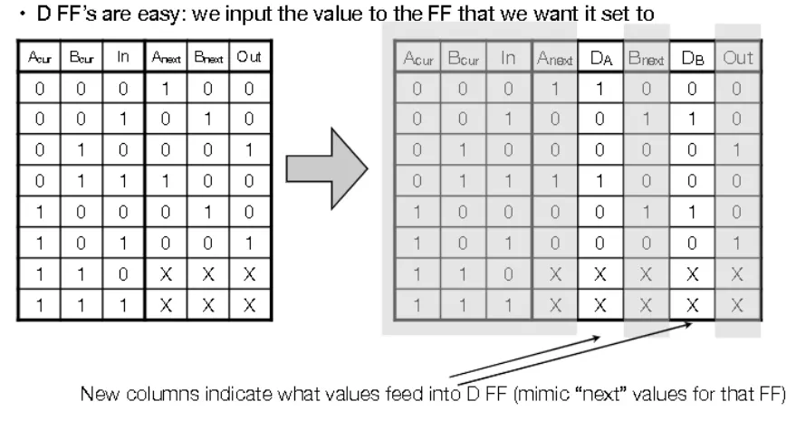
- To build state machine with flip flops, we need to figure out a map from the input column to the output column
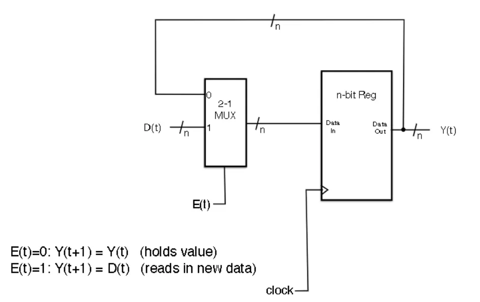
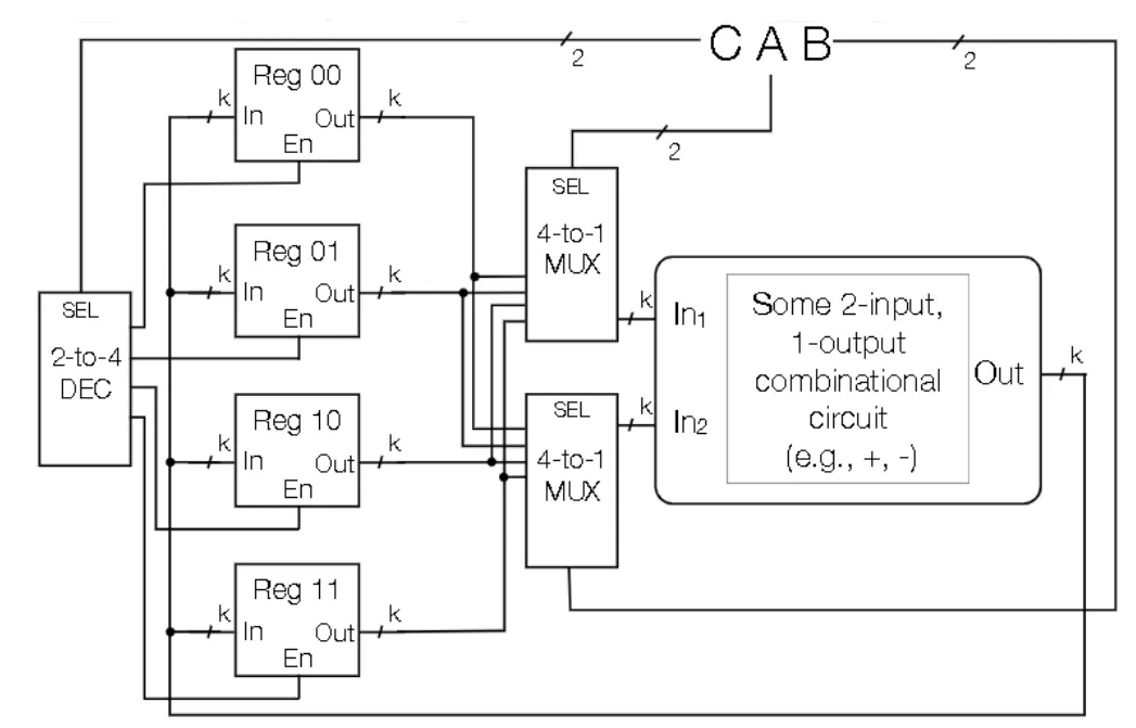
Registers
- A set of N flip flops that stores n bits in parallel
- The output of a register is the input from the previous cycle
- Can add Write Enable to command register to hold current value
- Setting enable states that you can now write to Register (Remember that you are always reading from all the registers at once, and you use a decoder to select which register values escape the register file)
- Implemented with a MUX
Register MUXing
- Decoder select which register is enabled
- MUXes determines which register gets fed into input
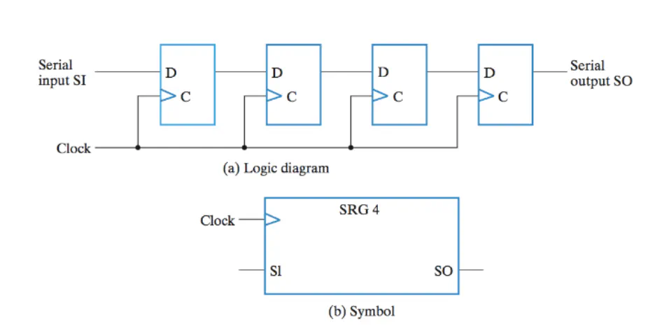
Shift Register
- Shift bits laterally in one direction
- Can be used to delay output by some number of clock cycles
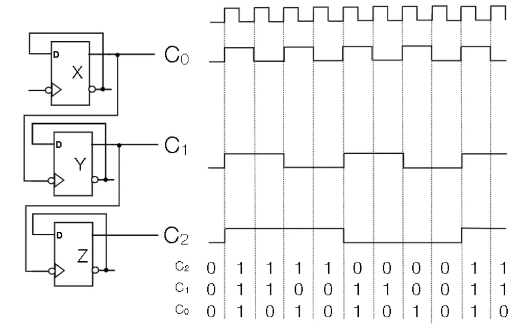
Ripple Counter
- The output of a flip flop is fed as the clock input to another flip flop. This can be daisy chained
- The output of C0 is half the rate of the clock. The output of C1 is half the rate of C1. This effectively creates a counter
- Can also implement a counter without daisy chaining (called Serial Counter)
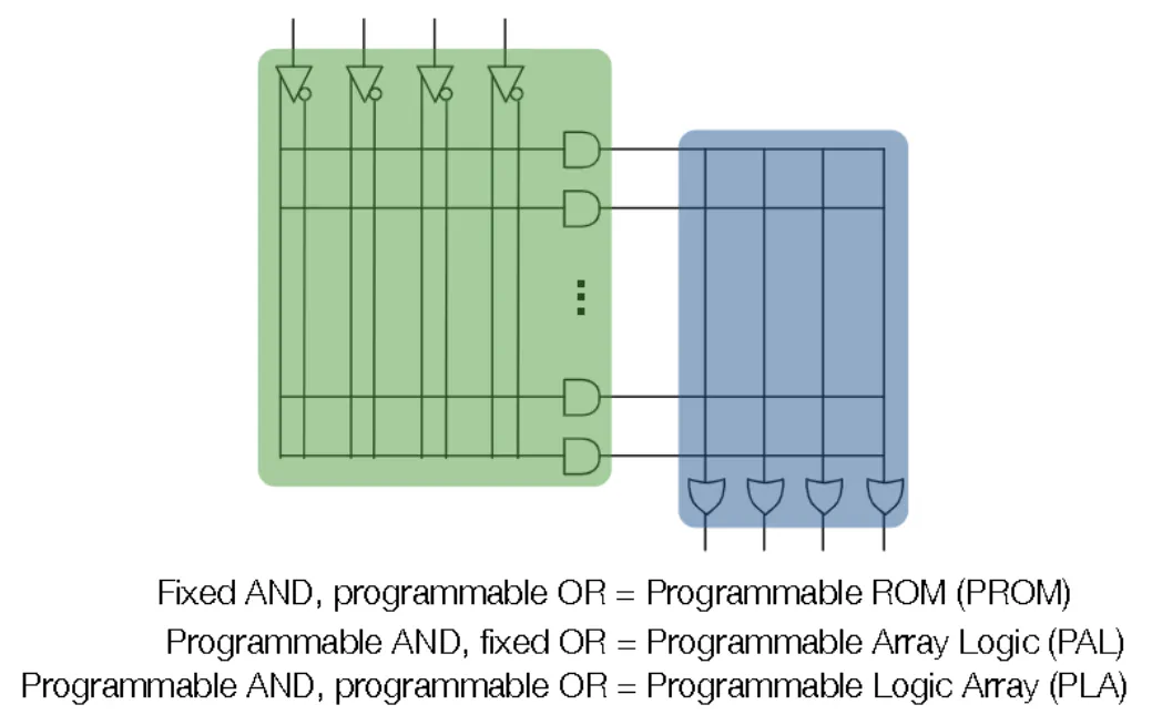
PLA (Programmable Logic Devices)
- Can select which wires connect to which gates with an X
MIPS Programming
- RISC = Reduced Instruction Set Computer
- MIPS (Microprocessor without Interlocked Pipeline Stages)
- Are “load-store” architectures where all operations are performed only on operands in registers, and we can only access memory via load and store
- CISC (Computer Instruction Set Computer) are architectures that are more complicated than this
Parts of a Program
- State: variables,arrays, and the raw text of the code
- Operation: compare values, make changes to state
- Control: Flow of program
Computer Hardware
CPU
- Control: tracks instruction to be executed in the current clock cycle
- Function Unit: Current function that you are doing
- Doesn’t hold onto output (Stateless)
- Takes in as input data and operation and outputs result of operation
- Register File: Collection of registers (except one called PC) that hold output of Function Unit
- Each register holds a word of k bits (for MIPS, we have 32 bits)
- Each register holds a word of data and has a unique name
- For MIPS, each register has an alpha numeric label that can be updated every clock cycle
- “Zero” register is always zero
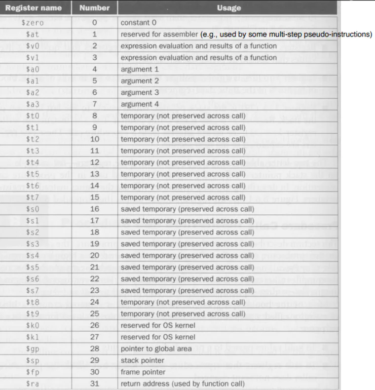
- Each register holds a word of k bits (for MIPS, we have 32 bits)
Memory
- Each address is associated with an 8 bit (1 byte) address
- You can retrieve a word by specifying the address that satisfied x mod 4 = 0. This selects this address and the next 3 addresses
Clock
- creates clock cycles that the computer uses to execute programs
ISA (Instruction Set Architecture)
- Interface between software and hardware
- set of operations (instructions)
- data units (sized, addressing modes, etc.)
- processor state (registers)
- input and output control (memory operations)
- execution model (program counter)
- For MIPS, everything is 32-bit
- Things that an Assembly Program can do:
- Read from register file
- Perform an operation
- Write to register file or memory
- Jump in program control
Programming in MIPS
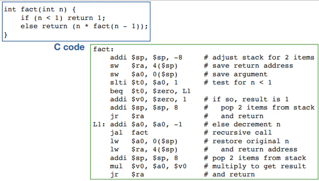
- Each line contains at most 1 instruction
- You can comment things with a #
- Each instruction consists of an op code and the associated parameters (ie. a series of registers and constants)
- Labels are used for control-oriented instructions and can either be on their own line or pre-appended to an instruction
Instruction Types
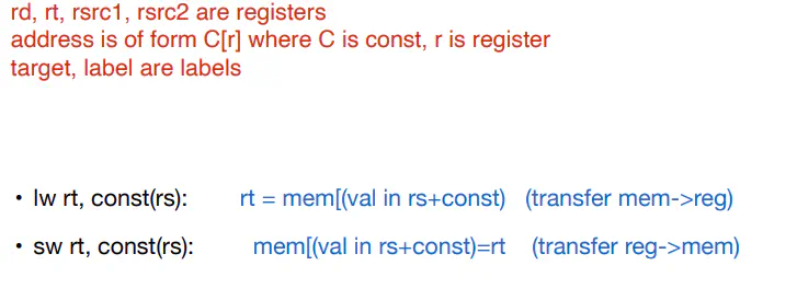
- Memory Access
- Arithmetic/Logic
- Jump/ Jump Subroutine/ Jump Return
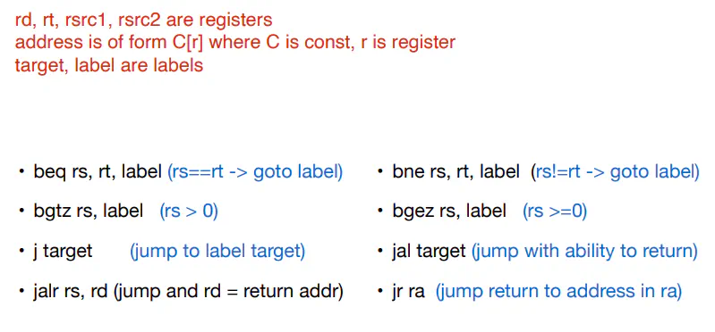
- Jump is an unconditional jump to an address in instruction memory
- Jal puts next instruction address in $ra and then jumps to the label
- jr Copied $ra into PC
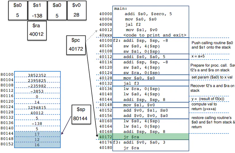
Memory Pointers
$pc
- register points to a memory address that holds the instruction to be run on the current clock cycle
- Normally, $pc gets incremented by 4 to go to the next instruction. Branches and jumps can go to any label
sp
- $sp register points to a memory address that is at the top of the stack
- Whenever you add or remove data from the stack, you decrement or increment the stack by 4 respectively
- Pushing is writing to the current address and then decrementing the stack by 4
- Popping is reading the current address and then incrementing the stack by 4
- Whenever you add or remove data from the stack, you decrement or increment the stack by 4 respectively
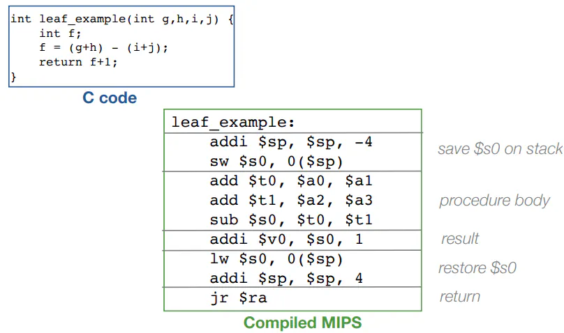
- leaf procedure is a procedure that does not call another function
- stack is used to save previous value of functions with the same names (ie f in a local function and f in main)
Constants
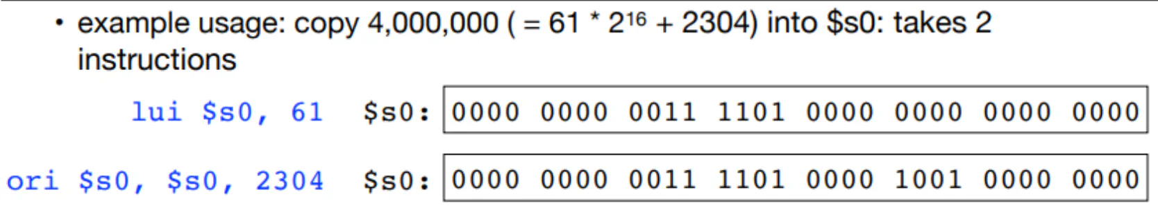
- MIPS uses 16 bits for constants
- 16 bits for the constant value. 16 bits on the instruction to use the value
Sign-extend
- Convert an unsigned N-bit to unsigned 2N-bit, pad with 0s to the left
- Covert signed N-bit to unsigned 2N bit
- Add 1’s if N-bit is negative
- Add 0’s if N-bit is positive
Pseudoinstructions
- Instructions that can be interpreted by the assembler, but is converted to other instructions beforehand
- Ex: move $t0\ $t1 becomes add $t0\ $zero $t1
Things to Remember
- Word addresses are not at sequential addresses. need to increment by 4, not 1
- Keep a pointer to an automatic variable (on the stack) after procedure returns
- Don’t modify things on the stacks
- Branches use indirect labelling (move 3 instructions forward) while Jumps use direct labelling (go to instruction at address 40,000)
Assembly Code
- 32 bit instructions
- First 6 bits are op codes, which tells you how to interpret the remaining bits
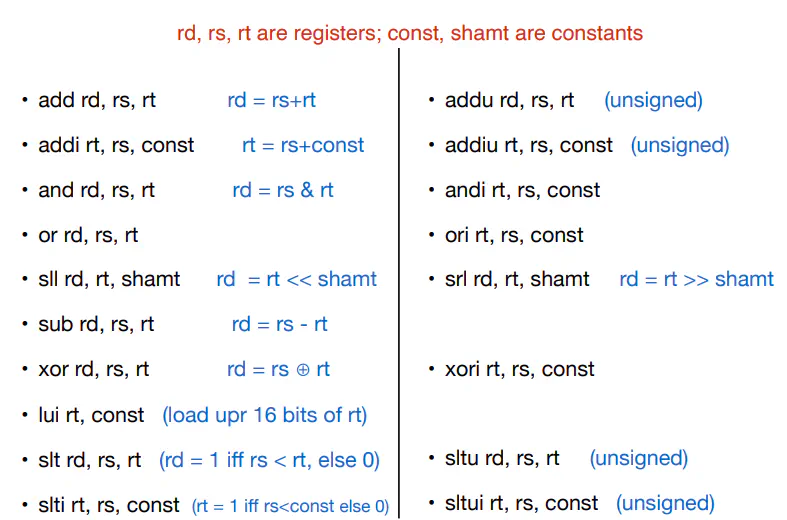
- 3 formats
- R-format: instruction with 3 register parameters
- Shifting is also R-formatted
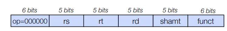
- op code is always 000000
- rs = 5-bit description of 1st register to be read from
- rt = 5-bit description of 2nd register to be read from
- rd = 5-bit description of register to be written to
- shamt: only used with shift op codes. Specification on how much to shift by
- funct: specific operation to be performed
- I-format/mem-access/conditional branches
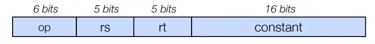
- op codes
- 1?????: memory access
- 001???: immediate arithmetic/logic op (uses a constant)
- 0001?? or 000001: conditional branch
- rs = 5-bit description of register to be read from
- rt = 5-bit description of 2nd register
- constant = 16-bit constant (usually signed)
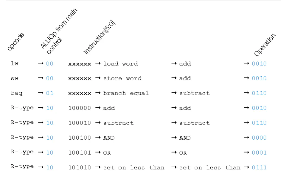
ALU
- Function unit that implements logic and arithmetic operations
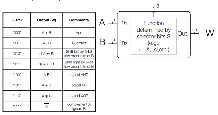
- XY is 00 and Z selects add or subtract
- Utilizes Circuitry mentioned in previous lectures
- XY is 00 and Z selects add or subtract
Details of Memory
- General Memory Interface
- k bit addresses ($2^k$ addresses), n-bit data
- Reading
- Specify k-bit address A
- Data-Out outputs the n-bit contents in memory at address A
- Ignores Data-In while reading
- Writing
- Specify a k-bit address A
- Through Data-In supply n-bit data to write at address A
- set Write-Enable to 1
- This outputs the value at the address until the value stabilizes. Can ignore output when writing
- NOTE: This can read and write at the same time
- Memory Internal Circuitry
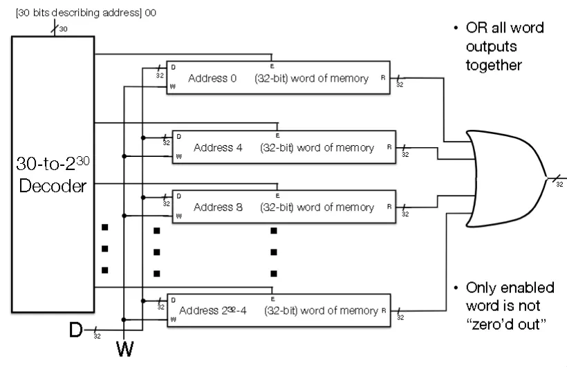
Single Memory Cell
- Setting E=0 doesn’t erase the value in latch, just “zeros” the value being output
- For MIPS, need to work with either all 32 bits of a word or none of them
- In other words, you enable 32 bits at a time
Coincident Selection
- 1D
- 1 Decoder
- k selector pins on decoder
- $2^k$ output pins
- For MIPS, we have k=30 because the lowest order bits are always 0
- Depth is $\log_2k+k$
- 2D
- 2 Decoders (1 for rows and 1 for columns)
- $k_1$ and $k_2$ selector pins where $k_1+k_2=k$, where k is the number of selector pins in 1D
- $2^{k_1}+2^{k_2}$ output pins
- Significantly fewer output pins
- Depth is max($\log_2k_1$,$\log_2k_1$)+2+k, which is comparable to 1D case
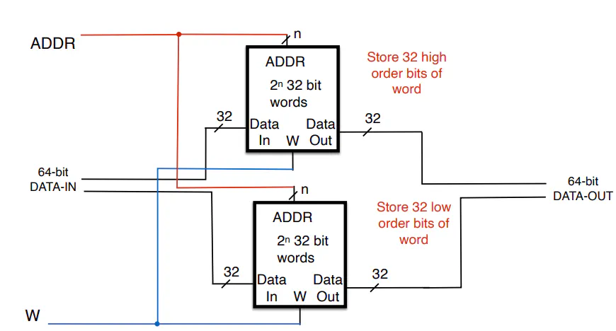
Extending Memory
- Extend word size
- Extend number of addresses
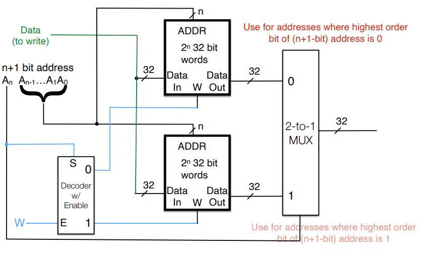
- Use highest order bit as selector in a mux
Why is memory not clocked?
- Memory is slower than everything else, so clocking it would slow things down
- Need to wait for an appropriate number of clock cycles for output and input to memory to stabilize
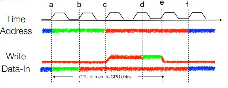
- Suppose you need 2 clock cycles to set an address, 1 cycle to prepare data for writing, and writing takes 1.5 cycles to ensure writing completed
- Green is correct value arrives, Red is correct value “stabilizes” in circuit, Blue is incorrect value for current write
Architectures
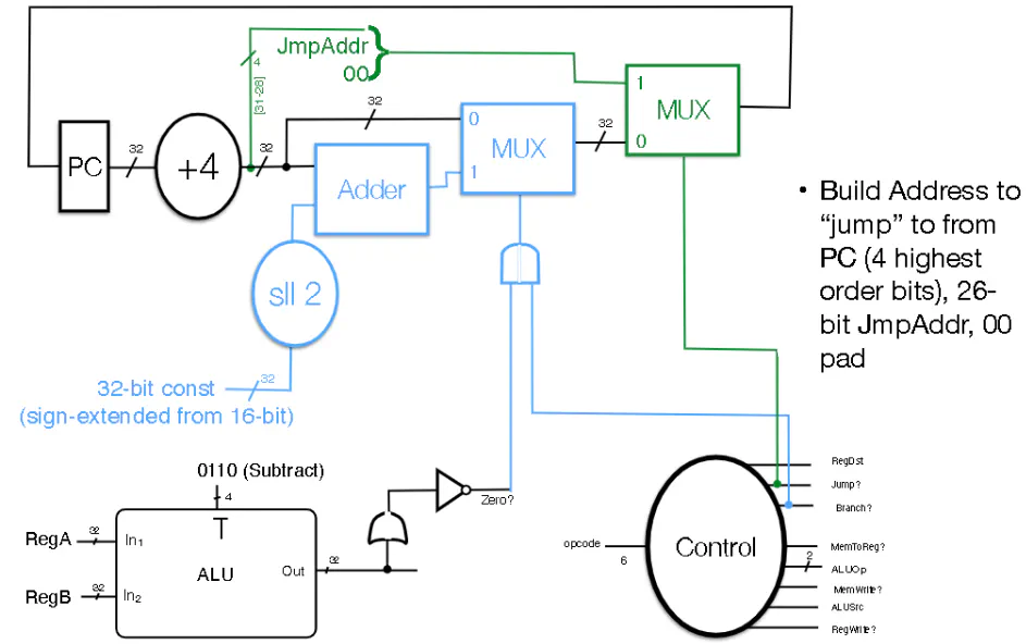
Single Cycle Architectures (SCA)
- Processes one instruction per cycle
- Two types of state: Data and Control
- Components
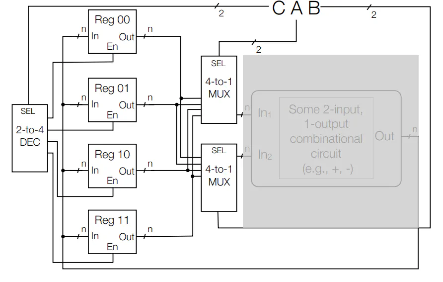
- Register files
- Series of Registers get feed into a series of MUXes and only a couple are chosen for computation and writing
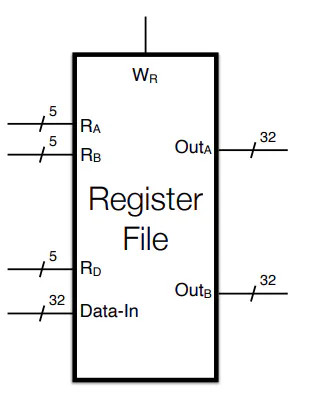
- $R_A,R_B$ are unsigned binary that describe which registers to read from
- $Out_A$ and $Out_B$ are the values in registers described above
- $R_D$ 5-bit description of a register to write to (if writing)
- $W_R$ writing flag
- Data-In: Data to write to R_D
- ALU
- Runs all possible computations simultaneously (all take the same amount of time) and only outputs what you need
- Memory
- Stores 32-bits at a time
- Two separate memories
- Instruction: Stores code to be executed
- Data: Stores program data
- Register files
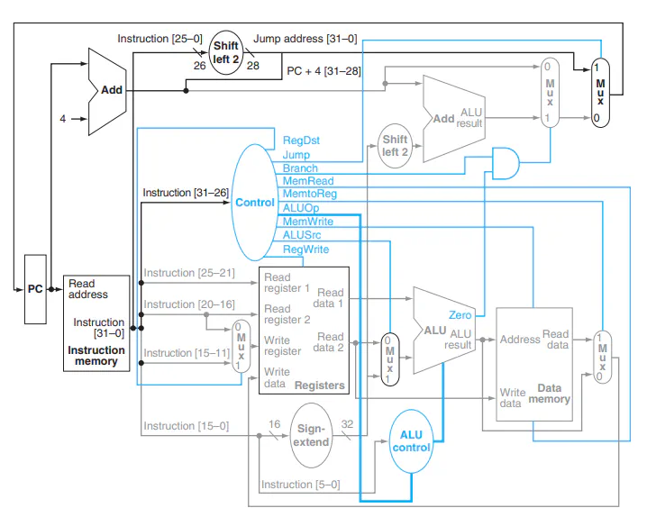
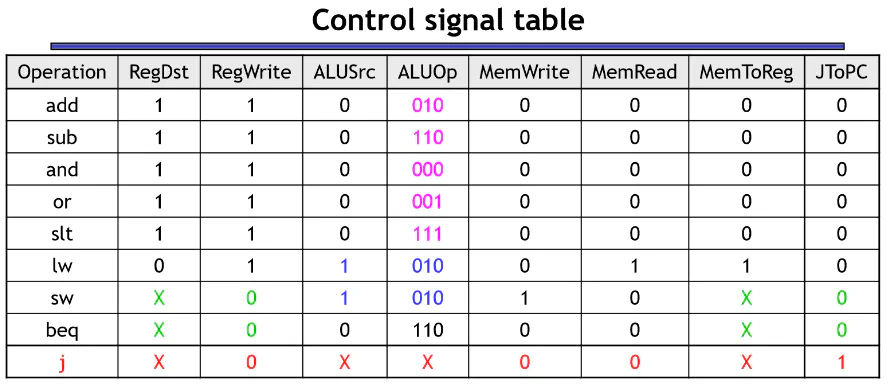
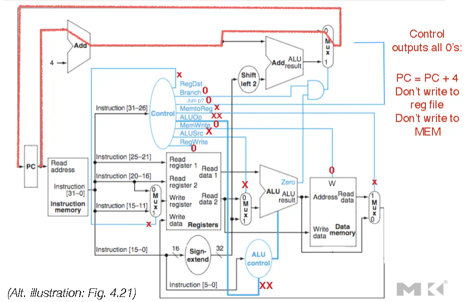
Control
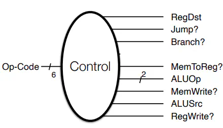
- RegDst: Whether RegA or RegD in the register file is written to
- Jump: Is this a Jump instruction?
- Branch: Is this a branch instruction?
- MemToReg: Will the output of memory be stored in a register
- ALUOp: Special Instructions for ALU
- MemWrite: Does this instruction write to memory
- ALUSrc: Is the ALU reading in a 2nd reg val or constant?
- RegWrite: Is the register file being written to?
- Just need to convert opcodes to truth table for each output of control. Straightforward, but tedious
- Just need to convert opcodes to truth table for each output of control. Straightforward, but tedious
Control Flow
Pipelines
- Main Idea: we break up instructions into smaller sub-tasks, then run these task in parallel
- Laundry Analogy:
- Suppose that Washing takes 30 min, Drying takes 45, Folding takes 30 and Putting things away takes 15. This takes at 2 hours if done sequentially
- If you run each tasks in parallel, each successive load takes more time to finish. However, the overall time needed to complete all your loads is less than running things sequentially
- You could also set at timer for the longest sub-task, and when you reach this time, you advance all your -sub-tasks to the next sub-task
- This takes longer than the previous version, but you aren’t switching between tasks as much
- Laundry Analogy:
- Summary:
- Single Cycle:
- Time to complete a single cycle is sum of sub-tasks
- Time to complete N tasks: N* sum of sub-tasks
- Compressed Pipeline:
- Time to complete a single cycle: growing
- Time to complete N tasks: sum of subtasks + (N-1)*longest sub-task
- Fixed Cycle:
- Time to complete a single cycle : k* longest sub-task
- Time to complete N tasks: N*sum of sub-tasks (N+k-1)*longest sub-task
- Single Cycle:
- NOTE: You are running at a faster clock cycle compared to single cycle
- You cannot skip steps in pipelining.
- For instance, say that you don’t want to fold your clothes, but other people do. You still need to wait for other people to finish
MIPS
- 5 stages: Instruction Fetch (IF), Instruction Decode (ID), Execute (EX), Memory (MEM), Write Back (WB)
- MIPS Pipelined Datapath
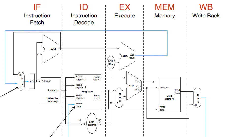
- IF Stage: Retrieves instruction from the Instruction Memory
- ID Stage: Decodes the instruction and pulls the appropriate registers
- EX Stage: Performs operations with the ALU and prepares for branching if needed
- MEM Stage: Write and read from memory if needed
- WB Stage: Write back output from memory to register file if Control says to do so
- Implemented via Pipeline Registers, which store the intermediate outputs of each stage for the later stage
- Can pass down any data from a stage (flags, outputs from ALU or memory etc.)
- Need to be large enough to store all the data flowwing through them (ie. each pipeline register is not the same size)
- Each Pipeline register passes down control signals until used, and then discards the used ones
- All instructions are read from Instruction memory in IF Stage
- R-type instructions pass through the entire pipeline like normal and then get written back if needed
- Branch and variant of jump are effectively done in ID stage. Afterwards, they move through the pipeline doing nothing
- EX and Mem stage are where the validity of Branch and Jump statements get evaluated and updated for PC respectively
- LW and Sw instructions are like R-type in that they only take effect in the WB stage
Dependencies
- Data Dependencies: Instruction B depends on the output of Instruction A when A changes the state of data to be used by B
- Control Dependencies: Instruction B depends on outcome of A (ie. B sometimes should not be run depending on the output of A)
Hazards
- A situation where an instruction entering the pipeline will be unable to correctly perform it’s intended function
- Structural Hazard: the instruction needs to use circuitry during a clock cycle while it is being used by another instruction
- Solution: replicate hardware (hence why there are separate memories for program and data)
- Data Hazard: the instruction will need access to data that is not available in permanent state (ie. register file or memory) during the required clock cycle
- Can partially be mitigated in register files by having the write phase happen on the first half of the clock cycle and have the read happen on the second half
- Implemented with more intermediate registers
- Can partially be mitigated in register files by having the write phase happen on the first half of the clock cycle and have the read happen on the second half
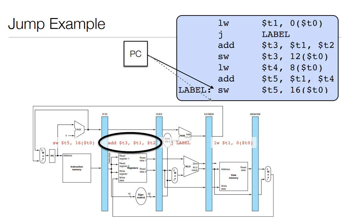
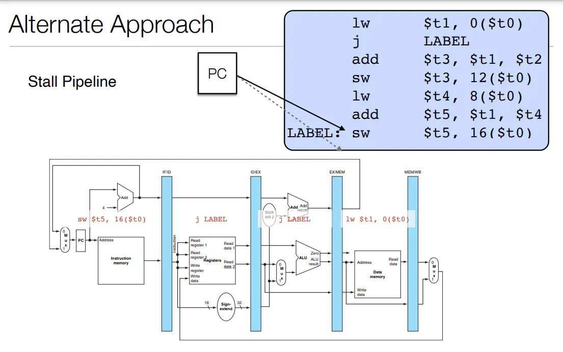
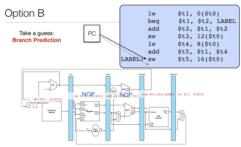
- Control Hazard: the instruction is not the correct instruction (doesn’t belong in the pipeline) or the system is unsure what instruction enters the pipeline next
- Structural Hazard: the instruction needs to use circuitry during a clock cycle while it is being used by another instruction
- To deal with Control and Structural Hazards, one way is via NOP instruction (do nothing except increment pc). This deals with the hazards, but partially destroys the advantage of pipelining
- NOPs means that the state of the CPU does not change. Hence NOPs disable writing to the register file and memory
- To deal with data hazards
- stalling (hold instruction until state is ready via NOPs)
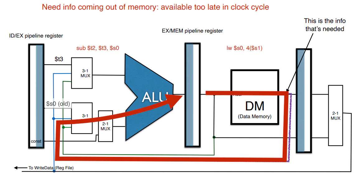
- data forwarding (forward information from past instructions to instruction creating the hazard)
- Alternatively, the necessary data for an instruction is already in the pipeline; hence the necessary data can be shuttled back in time
Implementing Hazard Correction
- Data Hazards
- stalling
- Hardware checks for data hazards, and then simultaneously runs an instruction again and sends a neutered version through the rest of the pipeline (ie. a modified instruction that does’t write to either memory or the register file)
- As long as instruction is cancelled prior to MEM and WB stages, then it is effectively voided
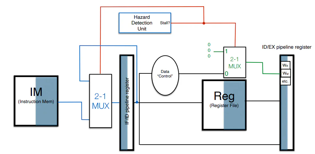
- Hardware checks for data hazards, and then simultaneously runs an instruction again and sends a neutered version through the rest of the pipeline (ie. a modified instruction that does’t write to either memory or the register file)
- data forwarding
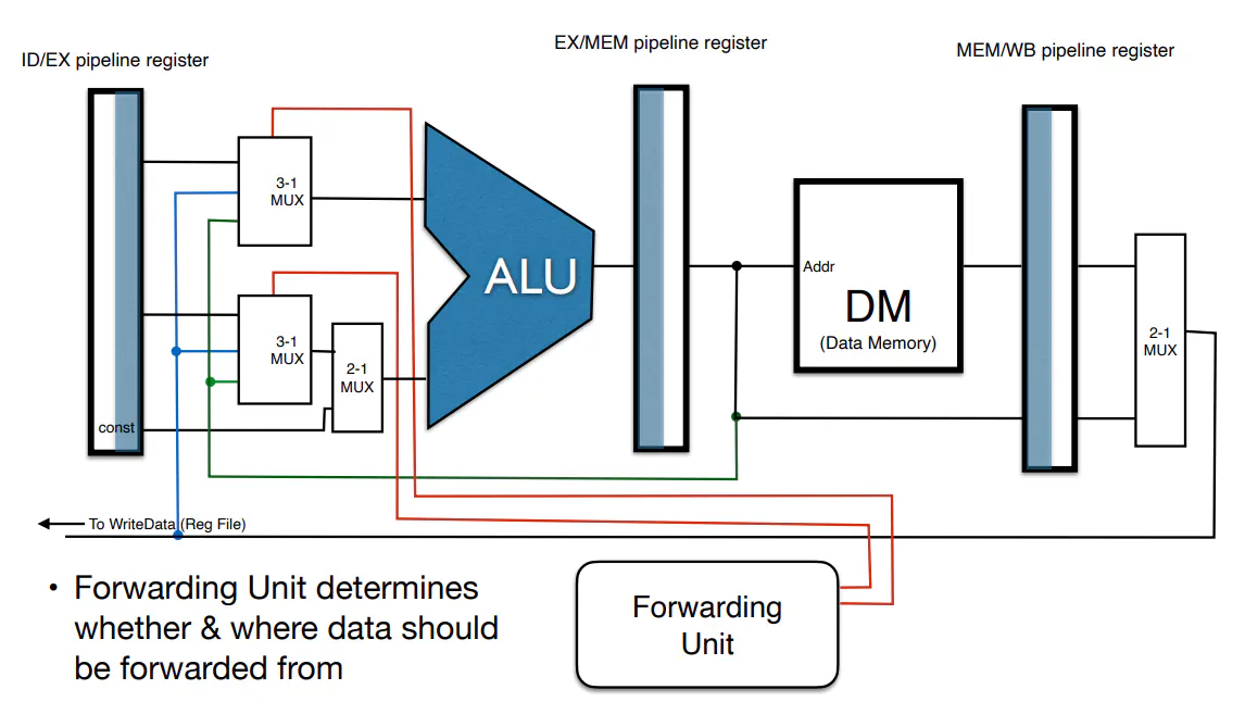
- However, stalls are still needed even with dataforwarding since dataforwarding might be too slow for some instructions
- Control Hazards
- branching:
- can either stall like data hazards
- Or you could predict (ie. make a guess about the what state we have and keep going. If we are incorrect, neuter the instructions that flowed through and update PC to correct location)
- can either stall like data hazards
Caching
- Memory Hierarchy (As you move from left to right, you increase in size and cost, and decrease in speed):
- Static RAM (SRAM: 1-5 ns), Dynamic RAM (DRAM 10 ns), Flash SSD (50 ns), Magnetic Disk (4000 ns)
- SRAM is what is used in Cache, DRAM is what is used in main memory, Flash is used for long term memory and Magnetic disks are pretty much obsolete except in niche edge cases
- The cache is a temporary copy of memory that can be read and written to much faster than main memory
- Used to store area of memory that are most frequently accessed (ie. we store areas of memory in cache to minimize fetches from and write to main memory)
- From the CPU perspective, it still appears that it is accessing main memory
Locality
- Temporal Locality: Items accesses recently are likely to be accessed again soon (ie. instructions in a for loop)
- Spatial Locality: Items near those accesses recently are likely to be accessed soon (ie. sequential instruction access, array data)
Blocks
- Blocks in cache refer to a fixed size unit of copying between cache and memory
- may consists of multiple words
- If a block is k-words long, then a cache miss causes a transfer of k words at once
- Block is to Word what Word is to Bytes in MIPS
Cache Hits and Misses
- A cache hit refers to any requests of the cache were the necessary data is present
- A cache miss refers to any requests of the cache where the necessary data is not present
- Miss penalty refers to the time required to copy the block from memory to the cache
- Miss ratio is the number of misses over the number of accesses
- On a cache hit, the the CPU proceeds as normal
- On a cache miss:
- The CPU pipeline gets stalled
- We fetch the correct block of memory
- After an instruction cache miss, restart instruction
- After a data cache miss, complete data access
- The challenges of Caching include:
- When to move data from memory to cache?
- How big of a blocksize should be used?
- Smaller means less unused stuff is moved
- It also means that separate moves are more costly (doesn’t take advantage of parallelism)
- For a fixed-sized cache, having larger blocks means that there are fewer block in total, which leads to more competition for fewer blocks, which leads to an increased miss rate
- The larger miss penalty could override the benefit of a reduced miss rate
- Where in cache to move fetched memory?
- Options include: least recently used, fixed mapping
- The overall goal is to minimize cache misses without spending too much time fetching unused data
Direct mapping
- A block lives in memory at a set of addresses, but may also be temporarily copied into the cache
- The block has a fixed location in the cache to which it can be copied (the block’s cache address)
- Since the cache is always smaller than the main memory, this create the problem where multiple blocks of main memory map to the same cache address. What differentiates different memory blocks?
- In addition to the k-word data block that is stored, you also store the “tag” of the block, which refers to the n-k highest order bits of the copied block of memory
- YOu also store a valid bit that is set to 1 if anything is written to a block. This takes into account cases where a cache block is initially empty
- As an example, look at a 32-bit memory address
- The 2 lowest order bits are the byte index into word
- The next n lowest order bits are the word index in a block (ie. A block consists of $2^n$ word)
- The next m lowest order bits are the block index within the cache (ie. a cache can consist of $2^m$ blocks)
- The remaining 32-n-2 bits are the tag
- In order to figure out in a particular memory address A is in the Cache, you first determine which block of memory this corresponds to, and then look for that block in the cache. You then check the tag of the cache block
- You can figure out the block address of memory address A by floor(A/k) where k is the block size
- You can figure out the block number via Block address modulo nb_cache, where nb_cache is the number of blocks in the cache
- You can figure out the tag just by right shifting the appropriate number of bits
Fully Associative Caching
- any block can go anywhere in cache
- Memory is still transferred in units of blocks
- You put the newly retrieved block in cache wherever you can based on some heuristic (put it in an empty block if you can, uses least accessed region of cache, or least frequently accessed region of cache)
- With Fully Associative, you are less likely to overwrite recently accessed memory locations, but you also incur a time penalty needed to locate a block in the cache
Set Associative Caching
- n-way associative: Given a M-block memory, a m-block cache that is n-way associative
- In general M*n/m blocks share cache locations
- A simple mapping implementing Set Associative Caching:
- Memory block i can map to memory block i% (m/n)+km/n for k = 0,1,2,…n-1
Writing to Main Memory
- Cache inconsistency refers to when data stored in a block of cache does not match data in memory (like after a sw command)
- Solutions include
- Write Through: On write, update memory as well as cache
- This would drastically slow down the speed, but this can be mitigates with a write buffer (ie. you store many write commands at once and only write when the buffer will overflow)
- Write Back: ON data-write hit, just update the block in cache memory
- Keep track of weather a block is “dirty” (ie. inconsistent with main memory)
- When you want to replace a dirty block, only then do you write the block to memory
- Can use a write buffer to allow replacing block to be read first
- Write Through: On write, update memory as well as cache
Virtual Memory
- All programs that are currently running cannot be stored in memory all at once
- Use disk space to store parts of memory used by a program while they are not being run
- When a program needs access to memory currently stored on disk, transfer from disk to memory