Notes adapted from MIT Digital Electronics Lab
Also from here
- Boolean Algebra Theorems
- Overview
Boolean Algebra Theorems
Let all variables be boolean in nature (ie. 0 or 1). $+$ Denotes an OR gate, and $\cdot$ denotes and AND gate
- $X+0 = X$
- $X\cdot 1 = X$
- $X+1 = 1$
- $X\dot 0 = 0$
- $X+X = X$
- $X\cdot X = X$
- $\bar{(\bar{X})} = X$
- $X+\bar{X} = 1$
- $X\cdot \bar{X} =0$
- $X+Y=Y+X$
- $X\cdot Y = Y\cdot X$
- $(X+Y)+Z = X+(Y+Z)$
- $(X\cdot Y) \cdot Z = X\cdot (Y\cdot Z)$
- $X\cdot(Y+Z) = (X \cdot Y) + (X \cdot Z)$
- $X+(Y\cdot Z) = (X + Y) \cdot (X + Z)$
- $X\cdot Y + X \cdot \bar{Y} = X$
- $ (X + Y) \cdot (X + \bar{Y}) = X$
- $X+X\cdot Y = X$
- $X\cdot (X + Y) = X$
- $(X+\bar{Y})\cdot Y = X \cdot Y$
- $(X\cdot \bar{Y}) + Y = X + Y$
- $(x \cdot Y)+(X\cdot Z) = X \cdot (Y+Z)$
- $(x + Y)\cdot (X + Z) = X + (Y \cdot Z)$
- $(X \cdot Y) + (Y \cdot Z) + (\bar{X} \cdot Z) = X\cdot Y + \bar{X}\cdot Z$
- $(X + Y) \cdot (Y + Z) \cdot (\bar{X} + Z) = (X + Y) \cdot (\bar{X} + Z)$
- $\overline{(X+Y+\dots)} = \bar{X} \cdot \bar{Y} \dots$
- $\overline{(X\cdot Y \cdot \dots)} = \bar{X} + \bar{Y} +\dots$
- Duality: The dual of an expression requires that you flip-flip $+$ with $\cdot$, flip flop 0 for 1, and leave all variables unchanged
Truth Tables
- You can use these rules to simplify boolean expressions, and then express the output of a boolean function in terms of a truth table
Specific Functions
1-Bit Functions
- Buffer: maintains the current input
- Inverter: Inverters the input
- Always On: always outputs 1, regardless of input
- Always Off: always outputs 0
2-bit Functions
- All standard logic gates are included here
XOR
- XOR can determine the sign of a multiplication if you let 0 mean positive and 1 mean negative. Then
- You can also think of A XOR B as doing the check A!=B
Overview
- Verilog is a Hardware description language which enables various levels of abstraction to describe underlying hardware (from highest to lowest)
- Behavioral/Algorithmic Level
- Dataflow level
- Gate level
- Switch level
- Only Behavioral and Dataflow are really feasible for actual designs
Verilog Basics
Variables
logicis one type of variable- Defaults to unsigned, 32 bit integers
- You can define the size of variables with the syntax [x:0]
- Make sure that you place the large number to the left
logic [3:0] a;
logic [11:0] b,c; // create many at once
- If you try and stuff a value which is too large, then the input will get truncated to fit (preserving the lsb’s first)
- Try to specify hardcoded values in the following format (why waste space if you ain’t using it?): S’Txxxx_xxxx
- S is the size of the number in bits
- ’ is the single quote
- T is the numberical base to use
- b for binary
- d for decimal
- h for hex
- xxxx_xxxx
- _ are ignored. Use for readability
- Each bit can either be:
- 0: logical 0
- 1: logical 1
- X: undefined
- Z: High Impedence (meaning it is driven by something else. Not commonly used)
- You can think of variables of multiple bits as arrays whose elements are 1 bit
- You can also create “2D” arrays
- a “packed” array has the elements be contiguous
- an “unpacked” doesn’t make this guarantee
logic [7:0] array4 [2:0]; //three 8 bit unpacked arrays (b[0] not contiguous with b[1])
// Can think of this as three 8-bit chunks
logic [2:0][7:0] array5 ; //three 8 bit packed arrays
//(array5[0] contiguous with array5[1])
// can think of this as one 24-bit chunk with sub-indexing syntax sugar
- Can use curly braces to pack variables together
logic [7:0] a, b;
assign a = 8;
assign b = 8;
logic [15:0] d;
assign d = {a,b};
- Ternary operators syntax is (condition)? happy_path: sad_path
logic [1:0] a, b;
a = b==2'b11? 2'b0: 2'b10;
Parameters
- can define as localparam or parameter
- localparam is not changeable
- parameter is changeable
localparam GOOD = 8'b1111_1111;
Operators and Loops
- Operators
- Follows C precedence
- Act on a variable level instead of a bit-level (in most cases. the Bit twiddling operators obviously act on only the bits)
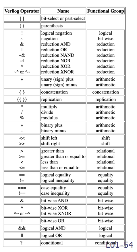
- Equality Checks: There are two types
- == compares 1’s to 0’s only
- === compares against all four types of possible bit values in an array
logic a,y;
initial begin
$display(5'b00001 == 8'b0000_00001); //eval to true
$display(5'b00001 === 8'b0000_00001); //eval to true
$display(5'b00001 == 8'b1000_0001); //eval to false!!
$display(5'b00001 === 8'b1000_0001); //eval to false!!
$display(a==y); //eval to undefined
$display(a===y); //eval to true (Since both are themselves X (undefined))
end
- Loops
- Think of Verilog for loops as loops in space, not loops in time!
- They are syntactical sugar to make laying out hardware easier
- Regular For Loop:
- If you are in an always block, you can use a four loop to replace a much of repetative lines
logic [63:0] a;
//assume b and c are large enough
always_comb begin
 for(integer i =0; i<64; i= i+1)begin
 a[i] = b[i]>c[63-i];
 end
end
- Generate for Loops
- Put for loops inside a generate block
- Useful if you need to
- Run multiple assign statements
- Create multiple always_comb, always_ff
- Create multiple instances of a module
- Create logics
- Need to use
genvarfor iterating variable instead of integer - Can label for loops to have access to inner constructions
generate
 genvar i;
 for(i=0; i<5; i=i+1)begin: myloop
 logic[31:0] hi;
 assign hi = 32'hAAAAAAAA ^ i;
 end
endgenerate
//outside of generate, those logics can be accessed with:
// myloop[2].hi for example
// this is needed since the logic hi needs more
// specificity than provided otherwise.
- Foor Loop Gotchas:
- Inside an always block, use a regular for loop
- If you want multiple assign or always-type blocks: use a generate loop
- The iterating variable used in a for loop has no hardware equivalent. It’s just a helper variable dduring specification
Enums
- You can define enums via
typedef enum {...,...,...} <enum_name>;
- Enums are typically assigns sequential from 0 onwards
- This behavior hand be changed to other encodings (johnson, gray, etc.)
typedef enum {IDLE,GOT_5c,GOT_10c,GOT_15c,GOT_20c,
 GOT_25c,GOT_35c,GOT_40c,GOT_45c,
 GOT_50c,RETURN_20c,RETURN_15c,
 RETURN_10c,RETURN_5c } state_enc_T;
(* fsm_encoding ="one_hot" *) state_enc_T state, next;```

### Design Rules

* Some of these won't make sense until you read the entire doc. Put here for easy access
* You should Design for Testing (DFT). Ie. Architect your system to give allow easier debugging
* Use hierarchical design: Things should be designed and tested in a modular fashion
* Use the same clock edge for all edge-triggered flip-flops
* Avoid implicit nets. Add "default_nettype none" directive to top of file to avoid inferring undeclared variables
  * Remember to reset default_nettype to wire, since some IPs require that
* Always assume that combinational logic glitches (ie. it may not always give you what you want)
  * Never clock a register from the output of a combinational logic
  * Never drive a critical control signal (such as write enable) frrom the output of combinational logic
  * Ensure that combinational logic is stable before it's sampled by CLK
  * Create glitch-free signals by
    * Registering outputs
    * Gating the clock
  * Avoid tri-state bus contention by design
  * Synchronize all asynchronous signals
    * Use two back to back registers
  * Use memory properly
    * avoid address changes when WE is true
    * Make sure write pulse is glitch free
  * Power supplies are noisy
    * Use bypass caps to filter noise
  * Chip-to-chip communication
    * There will be cross talk
    * Try synchronizing signals, or using async protocols

### Gotchas

* You don't typically need random access in arrays. FIFOs, queues, and other similar structures are normally sufficient and map closer to hardware
* Don't divide or do modulus unless absolutely necessary. These are horrendously inefficient on hardware
* Make sure that modules are mutually exclusive, collectively exhaustive
  * Branches should cover all seperate cases
  * All branches should need to output the same signals at the end of the logic chain
* Try and keep all signals clocked on the same clock unless absolutely necessary
  * If you need things to happen on the edge of a non-clock signal, keep track of the previous value
* Keep the number of clocks generated small

### Macros and Modules

* A particular board might have build in macros (ie. hardware devices) which you can map modules onto. Otherwise, verilog modules get synthesized based on some block allocation algorithm that the manufacturer decides

#### Declaring Modules

* Verilog uses a modules system. This can be some discrete element, or it can be a collection of lower level design blocks
* You can declare module as follows
module f1( input wire x, input wire y, input wire z, output logic output_1);
* You can declare an instance of a module via
  * Notice that you can specify which port to assign values to explicitly with the . notation
* Try and label inputs and outputs with _in and _out respectively
* Also, label inputs with type 'wire' since it will fully specify what type they are ('logic' can be ambiguous)
logic q,r,t,cat; //declare instance of that module: f1 my_f1(.x(q), .y(r), .z(t), .output_1(cat));
* Can add parameters to modules:
```verilog
module add_constant #(parameter TO_ADD = 12)
 (input wire [7:0] val_in, output logic [7:0] val_out);
 assign val_out = val_in + TO_ADD;
endmodule
// Specifying parameter value
add_constant #(.TO_ADD(5)) ac_1 (.val_in(c), .val_out(d));
Syntax Oddities
- Number specification notation: <size>’<base><number> where size denotes the number of bits, base denotes the base, and number is the value encoded in said base
- For instance, 4’b1010 if a 4-bit binary value, 16’h6cda is a 16 bit hex number, and 8’d40 is an 8-bit decimal value
- You can change utilize multi-bit signals with the [:] operator
- For instance, $input[7:0] a$ denotes an 8-bit input in little endian format (ie. the left is higher than the right)
- You can also add in some vector indicies before the variable name. This denotes the packing of the bits (so reg [7:0] mem [255:0]; denotes 256 elements, each of which is an 8-bit packed vector)
- You can also concatenate signals with {}
- assign {b[7:0],b[15:8]} = {a[15:8],a[7:0]}; is a byte swap
Combinational Logic
Continuous Assignment
-
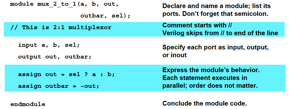
The above describes some basic features of Verilog
-
Inputs and outputs should be placed at the top of a module
-
You can use the assign keyword to continuously assign values to a variable
- You can think of this conceptually as continuously evaluating a function of arbitrarily changing inputs
- This lends itself very well to combinatorial logic
-
You can use the wire keyword to denotes connections between hardware elements (kind of like temporary variables?)
-
Can use ```always_comb begin … end`` unit to encapsulate more complex combinatorial logic
- Make sure you cover the entire input space!
- Use default and terminating else statements
- Look for inferred latches in the output of vivado
- Case statements: Can only be used inside always block
- use if pattern matching against a single variable
- Make sure that you always have a default case!
- There is no fall-through in Verilog, l=unlike C
- Don’t declare variables in always blocks
- Make sure you cover the entire input space!
-
There is also an
always @(sensitivity_list>) begin ... end. This was a general always block whose unction was inferred from the values in the sensitivity list
Procedural Assignment
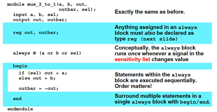
- You can procedurally assign values via initial and always blocks
- initial blocks cannot be synthesized, and are only used for simulation
- You must annotate values that get assigned in an always block with the reg keyword
- This tells Verilog that this value can change at any time, independently of any clock
You can mix and match procedural and continuous assignments
Glitches!
- Glitches arise in combinational circuits due to different propagation delays along the various branches
- You can’t avoid these. You can just minimize them…
- You can minimize glitches by “gating” the outputs of blocks with registers
- This add more latency, and takes up more space
- Hence, if you design in stages, you can focus on the propagation delays between modules, instead of how everything couples to everything else
Gotchas
- For combinational circuits, if a case is not specified, then the last value of the circuit gets latched and remains the output!
- Remember to precede all conditionals with a default assignment
- Or fully specify all branches of conditionals and assign all signals from all branches
- So for each if, include else
- For each case, include a default
- For if-else and case statements, make sure that each branch is mutually exclusive
- If you have a choice ,use a case statement over nested if-else, since that synthesizes to simpler logic
Nesting Modules
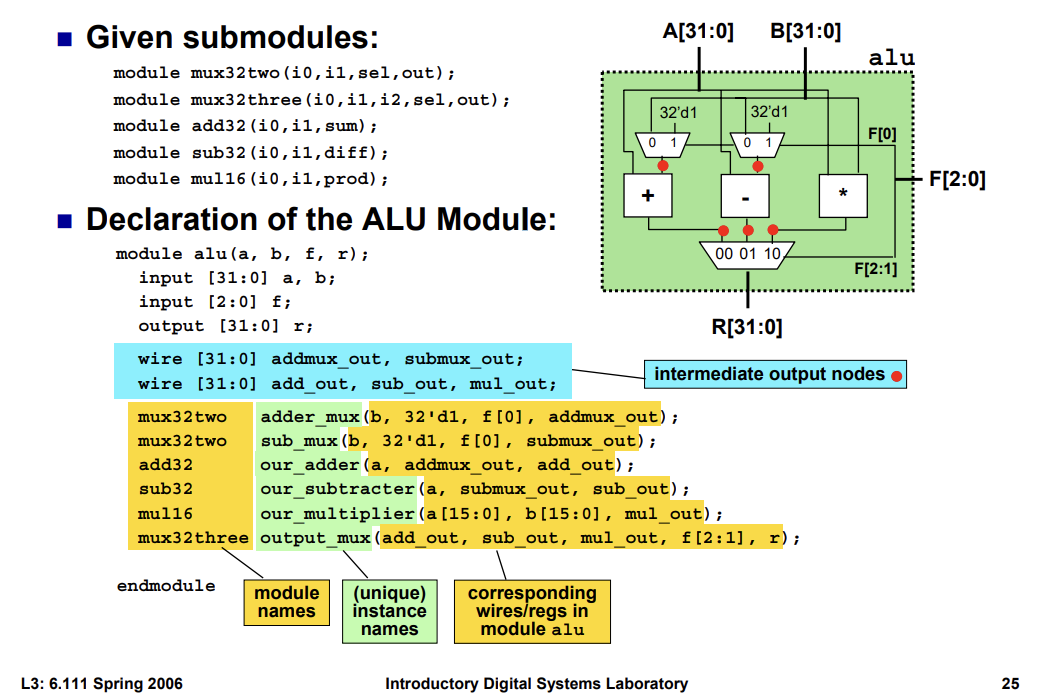
The above shows how you can compose modules from other modules. You need to specify the module name, give it a unique instance name, and then hook up the wires/registers of the modules appropriately

You can also specify the name of the input to allow better scaling of evolving design
Combinational Versus Sequential Logic
- For combinational logic, there is no memory of the past
- There is no feedback
- The output assumes that the implemented function that all transcients have died off
- Outputs can transition multiple times before settling to the correct value
- Sequential logic has memory, and is tied to a clock which keeps time
Latches
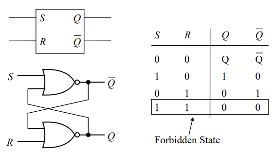
SR Latch is an implementation of a memory cell They are bi-stable and unclocked. They also have a forbidden state.
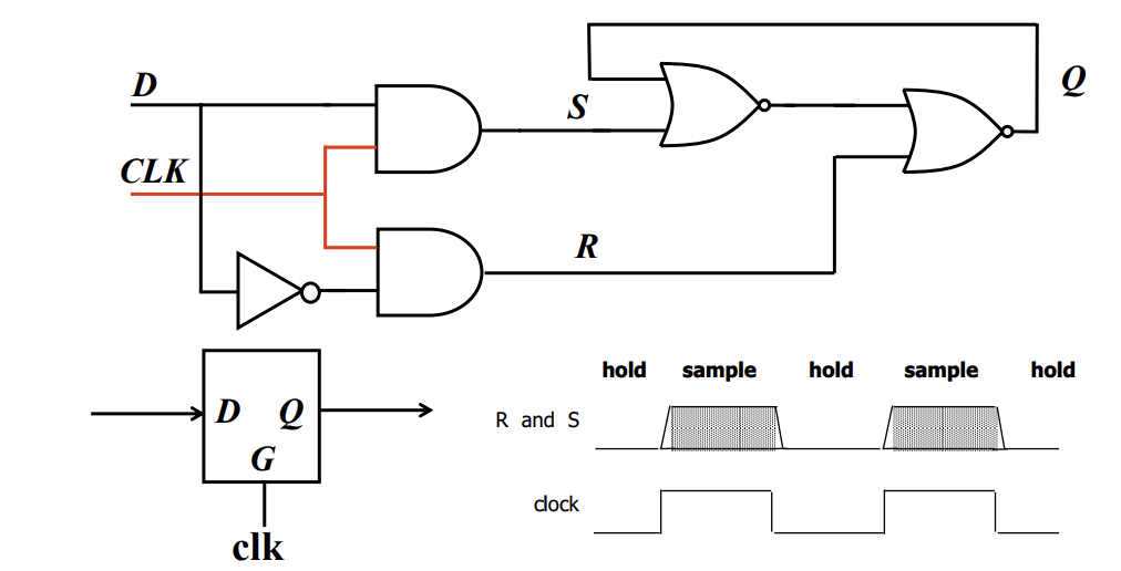
D Latch is an implementation that can be tied to a clock. The above is a positive D latch, which passes the D input to output Q when CLK is high. To invert this, simply invert the clock
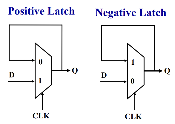
You could also do this funny thing where you use a multiplexer as a latch
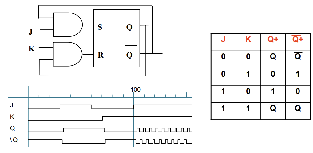
JK Latches eliminate the forbidden state by using feedback to ensure that both J and K can’t both be 1
Characteristic Equations

Registers
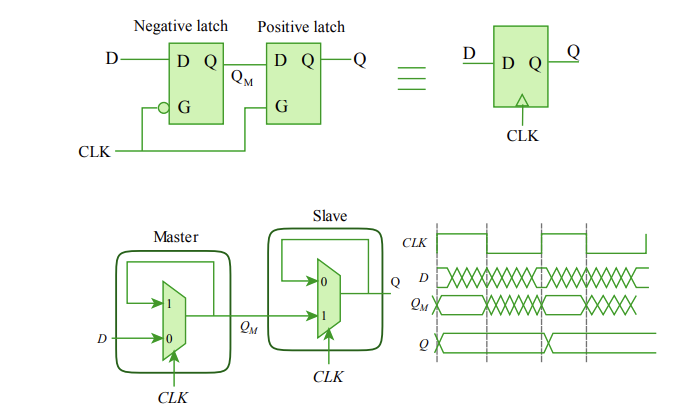
- The negative clock phase latches the inputs into the first latch
- The positive clock changes the output into the second latch
- Registers are different notationally from latches by a little triangle on the clock line
Registers can respond to clocks in several ways:
- They can be edge triggered, where the state changes on the pulse edge
- They can be level triggered/ transparent, where input gets sampled as long as the clock is asserted
- Both of the above can be either positive or negative
- Bubbles in IC diagrams represent a negative edge/level
Verilog for Sequential Blocks
- NOTE: Latches are almost never used by itself in a standard digital design flow. They quite often are inserted by mistake
- Try and feed a single global clock to all sequential elements
Sequential Always
-
The syntax is to use
always_ff @(trigger_type signal)to build using D-flip-flops (edge triggered sequential logic) or les commonly, to usealways_latchto build using D-latch- ’trigger_type’ denotes when the block gets run. Can be posedge and negedge
- ‘signal’ is the input clock signal
- You can chair triggers together. For instance: ‘always @ (negedge clearb or posedge clock)’
-
The old Verilog syntax is ‘always @ (’trigger_type’ ‘signal’)
- Ambiguous as to what will be generated (will it use flip-flops? latches? it’s case by case.)
- With always_ff and always_latch, the compiler will catch invalid usage earlier
- Ambiguous as to what will be generated (will it use flip-flops? latches? it’s case by case.)
-
When assigning in a sequential always block, make sure that you do it only once to avoid race conditions: always blocks execute in parallel
Blocking and Non-Blocking Assignment
- Blocking: use the normal ‘=’ operator inside always_comb
- This evaluates the expression and immediately assigns the value
- Non-blocking: use the ‘<=’ operators inside always_ff and always_latch
- This evaluates the expression, but defers the assignment to the end of the always block
- NOTE: Use nonblocking assignments for sequential always blocks, and blocking assignments for combinational logic
- Don’t mix blocking and nonblocking assignments in the same block
- If you are modelling sequential and “combinational” logic in the same always block, use nonblocking assignments
- Don’t make assignments to the same variable from more than one always block (normally throws errors, but might not if using blocking assignments)
External Signals (Metastability)
- External signals (like button presses) are not guaranteed to obey the timing requirements of the system
- You can solve a lot of problems by waiting for feeding the signal into exactly one flip-flop, and then waiting for the 1-2 clock cycles for the reading to no longer be metastable
- Depending on your signal, you might need more registers to reach stability
- Only use one chain of registers to handle metastablity. If you need asyncrhonouse input to branch out, do it after the single register chain
- This applies crossing clock domains: If you need to transfer a signal between domains, some chained registers are need to handle the metastable part
- You can solve a lot of problems by waiting for feeding the signal into exactly one flip-flop, and then waiting for the 1-2 clock cycles for the reading to no longer be metastable
FSMs
- Finite state machines output the output of the circuit and it’s next state at each clock edge
- Two types:
- Moore: output is purely a function of the state
- Mealy: output if a function of the state and the inputs
- You can convert a state transition diagram to truth tables and K maps in order to to translate state machines to hardware
- Mealy FSMs outputs generally occur one cycle earlier than a Moore
- Can think of FSMs as 4 parts:
- the current state
- the logic dictating the transition to the next state
- updating the current internal state
- outputting a value
FSM State Encoding
- Binary Encoding:
- For N states, there are ceil(log2(N)) bits, which each state getting a unique combination of bits
- One Hot:
- Each state gets its own bit in an N bit state vector
Converting to Verilog
- The state register of the FSM becomes a sequential always block
- the next state is a combinational always block with case statements
- The output logical block is a combinational always block or assign statements
- You can get glitches in output generation since FSM bits might not transition at precisely the same time
- To mitigate this, pass the combinational logic through a set of output registers
- This means that you calculate the output based on the next state
Clocks
- You can generate a clock signal a couple of ways
- A ring oscillator
- There are no stable states, and the period of oscillation is based on the delay of each element
- Crystal oscillators
- These are effectively high-Q LRC tank circuits
- It’s hard to break 200MHz with just crystals though. to go higher, we need frequency multipliers and PLLs
- Nexys4 boards have a clock wizard to generate other frequencies (ie. you provide the scaling factors and it generates the clock)
- A ring oscillator
PLLS
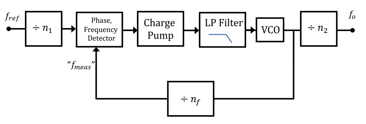
- VCOs are pretty simple to setup, but you can’t crank the voltage on them that high
- The phase lock loop tried to match the input phase to the measured output phase
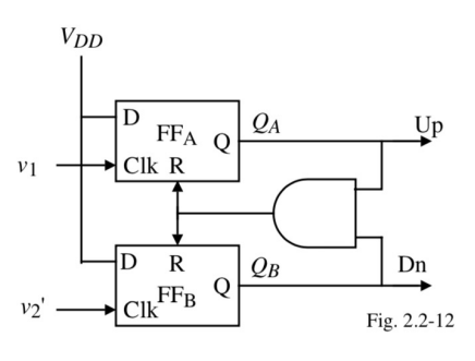
- The phase detector can be a simple XOR gate if you are close to the desired frequency, but a more robust approach is shown above.

- You can also think of the phase detector as a state machine
- If you are in state 0, then the clocks agree with each other
- If you are in state 1, then increase the voltage to the charge pump capacitor
- If you are in state 2, then decrease the voltage of the charge pump capacitor
- The Low pass filter kills of any annoying harmonics
- The divider blocks represent downshifting to lower frequencies.
- This “lies” to the phase frequency detector and drives the output more than normal, allowing output frequencies higher than the input
- Easiest divide is just by a power of 2 (negate clock signal only on certain edges)
- You can get other fractions by taking a weighted average of which power of 2 you use in a given instance
The Treachery of Clocks
- Clocks are not perfect
Skew
- Skew means that the arrival time of a clock signal at two different registers will differ due to finite speed of light
- based off of rising edges, not periods!
- Positive skew is when the first edge of a chain (launching edge) arrives before the second edge of a chain (receiving edge)
- Positive skew improves minimum cycle time of design,
- Negative skew is the other way around
Jitter
- The period of a clock can increase and decrease cycle to cycle
Proper usage
- Don’t utilize multiple clocks. Use one high speed clock, and then create enable signals only on a subset of edges
Timing
Timing Parameters
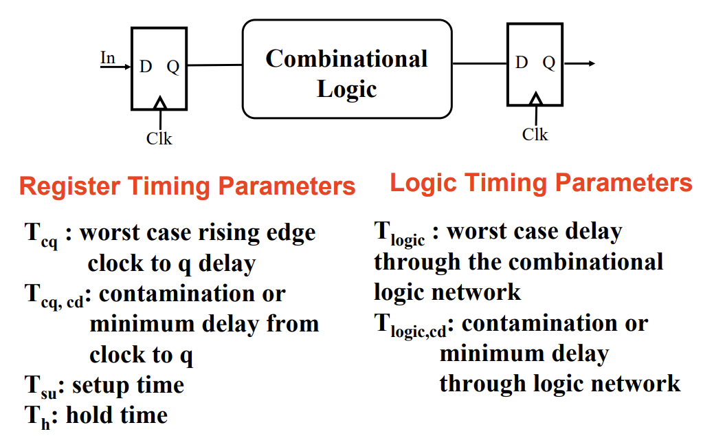
- You have certain coupling between these timing requirements:
- $T > T_{eq}+ T_{logic}+T_{su}$
- $T_{cq,cd} + T_{logic, cd}> T_{hold}$
- $t_{cd}$ states: How long before the system will start to respond at its output? (best case)
- If not specified, can assume it to be 0
- $t_{pd}$ states: How long until we can be sure the system has updated to a new value( worst case)
- If you encounter timing issues, you either need to reduce the propagation time of your circuit, or reduce your clock to accomodate the higher latency
Slack
- Slack is the metric of how safe your timing is
- Setup slack is time required to setup minus the actual setup time
- Hold slack is the actual time that a signal was held minus the required time the signal was held
- Both of these are defined such that Positive if GOOD, Negative is BAD
Video
- Humans can see about 10 million unique colors due to physical limitations
- An image is just an array of tuples of length 3, which represent RGB values
- Videos are just a bunch of images shown in rapid sucession
- Works because of the poor “RC time constants” of the human eye, which is a very funny EE joke
- We typically draw images/video with a raster pattern (sweep left to right, move down a line repeat until bottom, wrap around, repeat)
- Named after a Rastrum, used for musical staff drawing
- This allows us to encode 2D positional information (x0,y0) as a time
- original video involved 3 dimensions of information
- time conveyed x,y
- brightness (Lunimance) conveyed by amplitude
Black and White TV
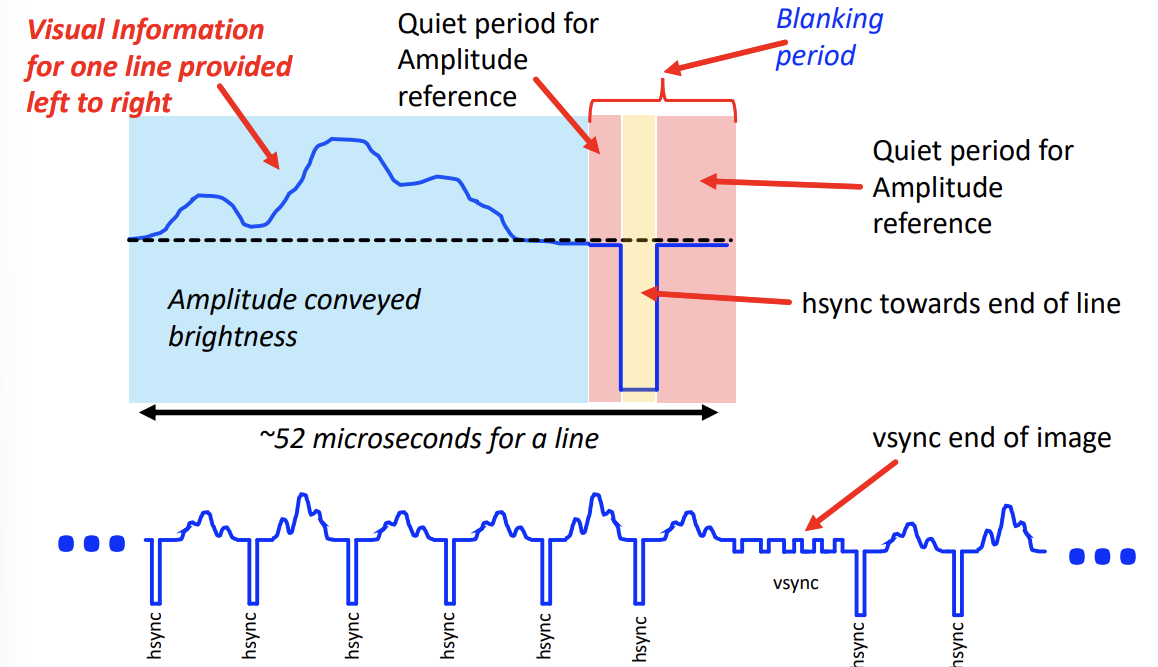
- Black and white video conveyed pixel information with the modulated wave
- The sync pulses also tells you when to roll over your counter and at what points you need to sample the waveform
- The quiet period(s) are needed to establish a baseline for the amplitude measurements
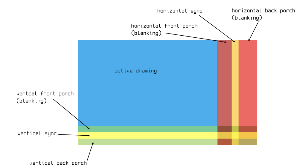
- Putting it all together, we have the full frame of information
- Some diagrams place sync portions elsewhere. Doesn’t matter in practice, since we are just sending serial data through a wire
Color TV
- To maintain backwards compatibility with B&W TVs, you still need to give a valid BW signal
- Enter YCrCb (Luminance, Red Chronimance, Blue Chrominance) space
- To convert between RGB and YCrCb, you just do some matrix multiplication
- This can be implemented with integer operators
- You can also use 5 BRAMs to store the necessary multiplications via lookup tables
- To make analog color (Called NTSC or composite video encoding):
- you superimpose the Cr and Cb signals as two amplitude modulated sine waves onto the Luminance signal
- You then add a “colorburst” signal in the back porch to define the frequency and reference amplitudes for the chrominance signals
- Combining the chrominance signals leads to another color space representation (HSL):
- The amplitude of the signal is now the Saturation
- The phase of the signal is the Hue
- The original Luminance value is the low low-frequency original value (use a low pass filter to extract)
- Fun cylindrical color space
VGA
- VGA is very similar to composite
- It has the same sync signals
- But now the RGD values are split out into 3 seperate signals instead of superimposed
HDMI
- Basic signals
- 3 differential pairs carry RGB information
- One wire carries the clock signal
- Data is sent in 10-bit frames using TMDS
- There is one pixel of info per clock cycle (the clock is 1/10 of the bit rate)
- The blue channel also (for backwards compatilibity reasons to VGA b/c of course) carries HSync and VSync signals. These are encoded as reserved 10 bit values
- (H = 0, V = 0): 1101010100
- (H = 1, V = 0): 0010101011
- (H = 1, V = 0): 0101010100
- (H = 1, V = 1): 1010101011
- Audio
- During the blanking periods, you shove audio information into the red and green channels (about 64 pixels per line)
- At 60 Hz, with 1080 lines per screen at 64 pixels per line, you get a audio rate of about 33 Mbps
- Super overkill for more audio applications
- Plenty of room for spyware
- TMDS
- Transition Minimizing: For 720p, we are sending 74 million pixels per second, and we need to send 8 bits serially for each channels. This means that each channel is pushing ~600 million bits per second, which causes lots of noise on the line due to rapid transitions
- Differential Signalling: This high frequency signal potentially needs to travel long distances. Using twisted pairs helps reduce the noise on the line
- Hence for HDMI, we send 10 bits instead of 8 bits in order to minimize transitions and let recovery circuitry to work on the receiver side
- Two ways of producing video
- Frame Buffers: Separate computation of drawing from actual drawing
- Racing the Beam: Everything runs off of the video timing signals
- You have each “sprite” on screen calculate it’s contribution to the current pixel being drawn, then logical or all of the signals together to produce the final output
Memory
- Access times of memory (ie. latencies) have not kept pace with cycle times
- So memory is often the bottleneck for a design
- Memory takes time to read and write at a hardware level (most software doesn’t care about this)
History of Memory
- Punch cards: switches detect holes in punch cards as 1’s and 0’s
- Drum Memory: Information stored magnetically on large rotating metallic cylinder (read-write, non-volatile)
- Delay Line Memory: You store data as sound waves in mercury (volatile, requires refresh circuitry, read/write)
- There were also mechanical delay line memories (ie. ones and zeros encoded as rotations of long wire)
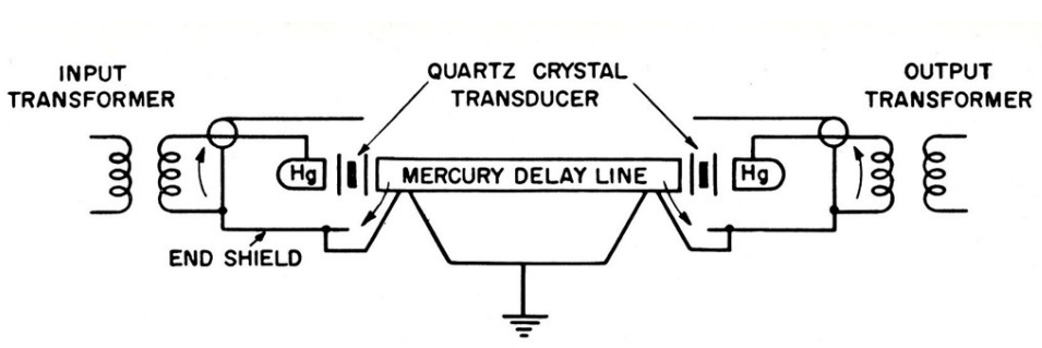
- There were also mechanical delay line memories (ie. ones and zeros encoded as rotations of long wire)
- William’s Tube: Use decay time of phosphors on CRT to store data (use camera as refresh circuitry)
- Core Memory: Store data in magnetic field of small torroids (non-volatile)
- The term core dump comes from these!
- Transistor based: Modern memory is based on this
Key parameters of memory
- Memory Density and Size
- High density memory rarely allows direct access (too many wires to be dense)
- To achieve high density, need to use row and columns
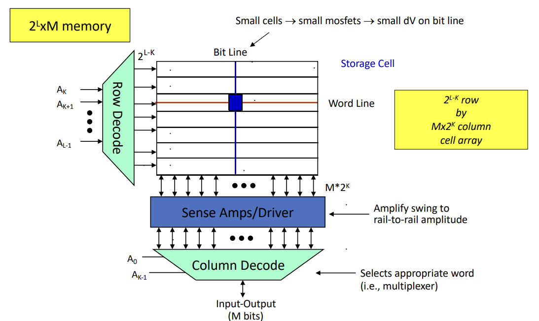
- With the right interfacing, you can treat this as a 1D array
- Because of this topology, you can’t access memory at multiple locations
- Also because of this topology, accessing adjacent addresses might be faster than reading distant addresses
- 3D memory allows much higher density of memory (access problem still persists)
- Access Time and Throughput
- Power Dissipation
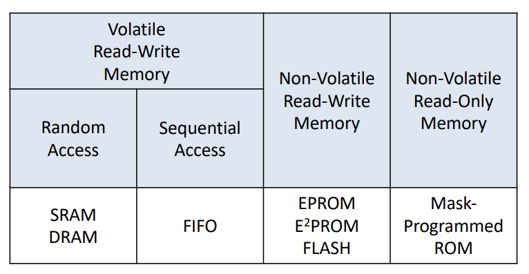
- Random Access: Given any address, get corresponding data. Access does not need to be in order
- Sequential Access: Put in values in a particular order, get them out in the same order
- Can’t get or modify values at will. Need to wait for appropriate values
FPGA SRAM Fabric
- On the FPGA fabric, memory consists of SRAM and Flip-Flips
- Flip-flops are evenly distributed throughout the fabric, and are not meant to store large chunks of memory
- A SRAM Cell (6-T Cell)
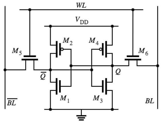
- State held by cross-coupled inverters
- Feedback must be overdriven to write into memory
- Write: Drive BL and $\bar{BL}$, then enable WL
- Read: Disconnect BL and $\bar{BL}$, then enable WL
- SRAM on FPGAs are also subdivided into two:
- Block RAM (BRAM)
- Contiguous chunks of memory
- Can’t provide asynchronous reads. You can get sketchy synchronous reads with a one-clock cycle delay (should do two-cycle delays though)
- There is no single cycle bulk reset
- Useful from clock domain crossing:
- Write with on clock onto port A, read with a different clock on Port B
- Distributed RAM (9,600 LUTs with 64 bits of SRAM)
- LUTs (lookup tables): Can synthesize any six-input loopup table/K-map/function
- For normal programs, you just set the SRAM once and treat it as ROM
- To use this SRAM as generic memory, just change it over time
- Gives single cycle read/writes, and you can read multiple values at once
- Use for small memory
- Difficult to route is heavily utilized
- Block RAM (BRAM)
Case Studies
- What memory your logic gets assigned to depends on how you write your Verilog
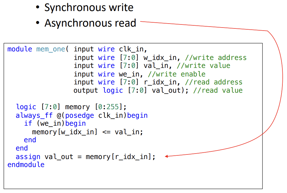
- This gets put into distributed SRAM
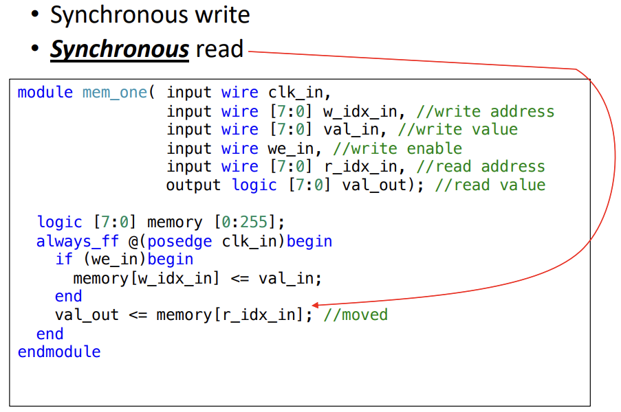
- This gets put in BRAM, since sync reads are impossible
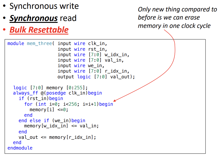
- This gets shoved into the Flip Flops, which is bad bc that takes away from the rest of your design
- Try to stick with standard verilog templates
Off FPGA Memory
EPROM Family
- EPROM, EEPROM, Flash (and SSDs)
- Use Floating Gates
- Uses high voltage (12V over nms) to tunnel electrons in and out
- Causes massive wear and tear (100,000 cycles)
- Mitigates by wear leveling
- Non-volatile
- Slow write speeds, fast reads
- Use Floating Gates
- FPGA typically has some external flash chip on the board, and can interface with external SD cards
DRAM
-
Dynamic random access memory
-
DRAM has single transistor and capacitor per cell (capacitor stores the state!)
- This allows really high density memory
-
Variables access times, but reasonably fast (50-250 ns)
-
Need to be refreshed constantly b/c capacitors don’t hold charge for long
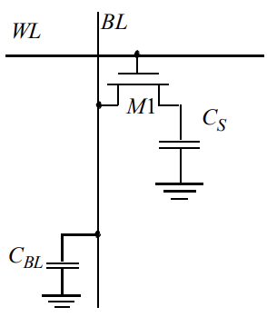
- To write: Set BL, then enable WL (set to $V_{DD}$)
- To read: set BL to $V_{dd}/2$, then enable WL
- Reading is destructive, since we need to bleed the capacitor off (you need to write back what you read). This refresh rate is around 100 ms
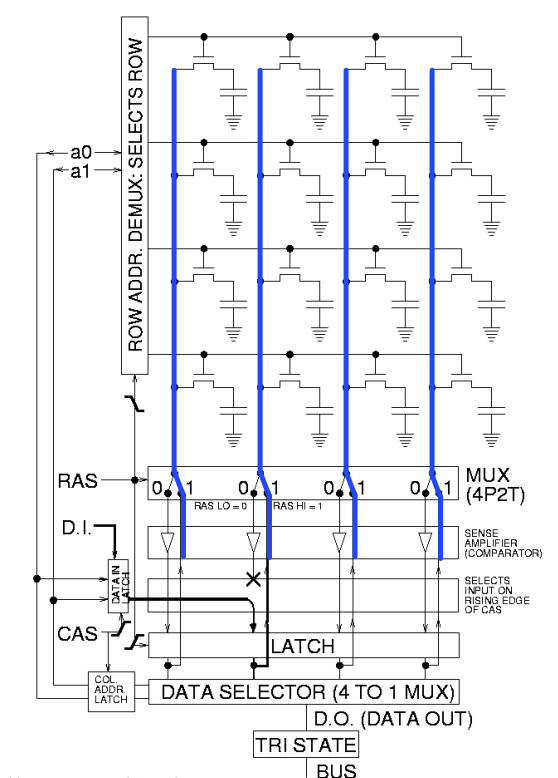
- Reading is destructive, since we need to bleed the capacitor off (you need to write back what you read). This refresh rate is around 100 ms
-
There are so many flavors of DRAM
- DRAM (Async)
- SDRAM (Synchronous DRAM)
- 1 Clock cycle per operation
- Single Data Rate SDRAM (SDR SDRAM)
- One R/W per clock Cycle
- Double-Data Rate SDRAM (DDR SDRAM)
- Two R/W per clock cycle
- Higher speed DRAM (DDR2, DDR3)
- Lower voltage/higher clock variants (LD…)
-
To interface, use the Memory Interface Generator (MIG) provided by the vendor, so you don’t have to write the Verilog code to implement this
-
The usage of DDR is either
- LOTs of data needed in random access at medium data rates
- ~100 MBytes/s average R/W
- MASSIVE amounts of data needed in short, high speed bursts
- ~ 1.2 Gbytes/s in small bursts
- LOTs of data needed in random access at medium data rates
Buffering DRAM
- Since DRAM response times are variable (due to the whole refreshing thing), you don’t know when you will get a response
- Hence, you typically surround DRAM with some buffers in order to not deal with that
- One structure is a FIFO (First In, First Out)
- Can implement in Distributed SRAM, or BRAM
- In BRAM, can use the two ports to read/write to different SRAM cells at the same time. With some wrapper logic, this can be a FIFO
- Do this FIFO wrapping whenever you have two modules which share data, but they produce/consume data at different rates
FSM Modularization
- You can encapsulate subtasks as minor FSMs within a Major FSM, and have a common reset and clock
- You have an input START wire, and an output BUSY wire
- START tells you when to run a FSM
- BUSY tells you when the FSM work is done (or sometimes, a 1 cycle DONE signal)
- This abstraction is useful for
- Modular design
- Recurring tasks in different contexts
- Tasks of variable/unknown periods of time
- Event-driven systems
- You can optimize this setup by de-asserting the busy signal one state earlier
- Be careful that the last state only lasts one cyclem otherwise, you can get stuck
Pipelining
- Latency (L): time between arrival of new input and generation of corresponding output
- For purely combinational circuits, this is just $t_{pd}$
- Throughput (T): rate at which new outputs appear
- For purely combinational circuits, this is just $\frac{1}{t_{pd}}$
- For purely combinational circuits, sometimes an earlier stage might finish sooner than a later state
- Adding a register between these stages of different times allows earlier stages to take in more data
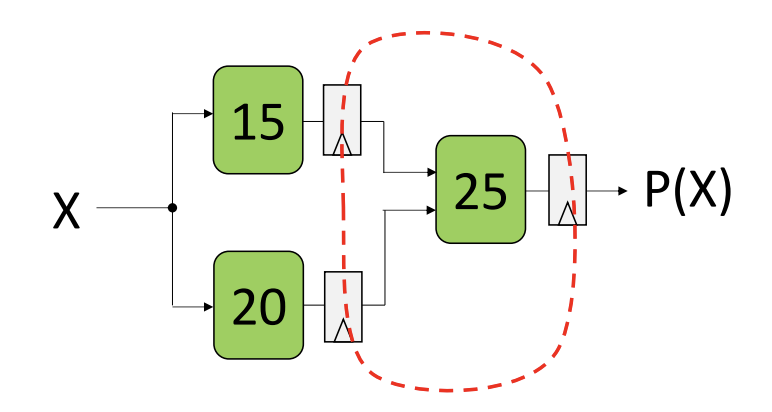
- Adding a register between these stages of different times allows earlier stages to take in more data
- A K-stage Pipeline is an acyclic circuit having exactly K registers on EVERY path from an input to an output
- A purely combinational circuit is a 0-stage Pipeline
- Conventionally, every pipeline stage has a register on its OUTPUT, not it’s input
- The clock period must satisfy the following equation: $t_{PD, reg1}+t_{PD,logic}+t_{SETUP, reg2} \leq t_{CLK}$
- In words, the clock period must be greater than the logic time, the propagation time of reg1, and the setup time of reg2
- Latency if a K-pipeline is K times the common clock period
- Throughput of a K-pipeline is the frequency of the clock
- To pipeline a system:
- Start at the output, and add a register there
- From the register, draw a contour backwards taht includes as much of the circuit that will fit inside required the required period. Add resisters at these intersections
- Repeat until throughput is good enough. Look for redundant registers
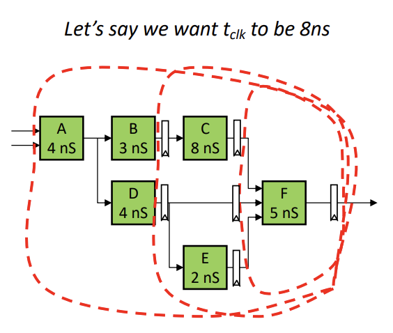
- In verilog, this just means adding some intermediate always_ff blocks to your code (remember metastability solution!)
- Pipelining slows things down, but makes sure everything is synchronized
- Only as good as the weakest (or in this case, slowest) link
Math Complexity
- Addition: Ripple Carry, which is a bunch of cascaded Full adder blocks
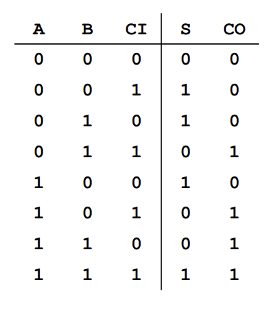
- Recall $-B = ~B+1$ in twos complement. So Subtraction can be represented by Addition
- Worst case propagation time is if a carry bit goes from LSB to Mbps
- $t_{adder} = (N-1)t_{carry}+t_{sum}$
- Can mitigate this with carry-look-ahead adder
- Adding and subtracting are fast (32 bit add can be done in a clock cycle easy)
- Don’t stack too many though, since built in logic slices on board have limitations
- Nested if-else statements can cause propagation delays
- Use case statements if priority doesn’t matter
- Also remember that branching logic inside if-else can cause propagation delays as well
- Multiplication is more intensive than addition, so if possible, try to use bit shifts
- FPGA has built in hardware multiplier modules called DSP48 blocks, which are capable of single cycle multiplication
- At 100 MHz, about one 32-bit multiply per clock cycle is feasible (will use several DSPs though)
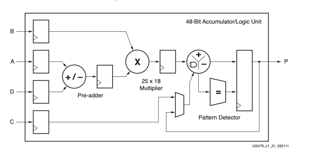
- Division is hard. Like, significantly hard than the rest. Try to right shift if possbile
- If you must divide, realize that it ain’t happening on one clock cycle
- Same for square root, cosine, etc. If you need a value fast, you use a lookup table, which trades speed for memory
Division
- Below shows an example division algorithm which spreads the computation over an unknown number of clock cycles (ie. implement this as a FSM)
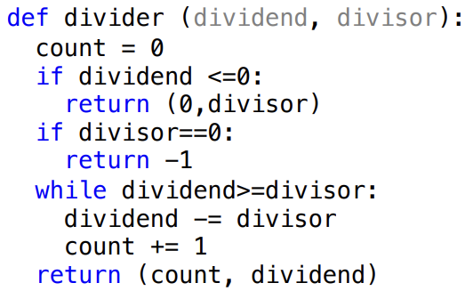
- The good
- It meets the timing requirements
- The bad
- It’s a blocking implementation (low and variable throughput)
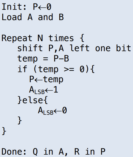
- Above shows an algorithm which takes a fixed number of steps (but it’s still blocking though)
- Assume that the Dividend A and the divisor B and N bits
- In words, it creates a sequential circuits to process one subtraction, then repeats N times
- Only works for signed operands. For unsigned, just remember sign of inputs and tack on at the end of the computation
- The good
- Meets timing
- Same resource usage as one
- Fixed cycle runtime
- The back
- Blocking implementation (low-throughput)
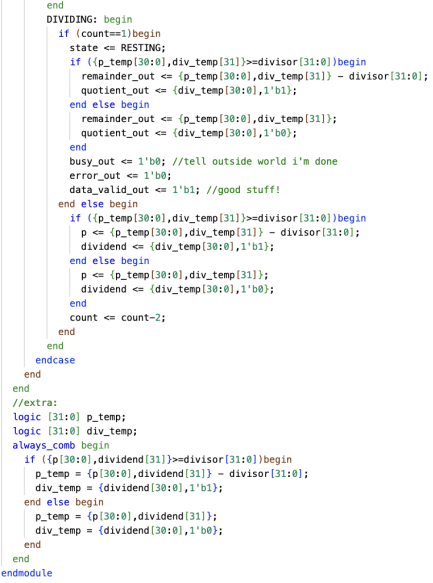
Could try to add an additional subtraction per cycle
-
Uses an seperate always_comb block with some temp variables to perform the second iteration
-
With the fixed cycle number algorithm, we can try and pipeline the procedure
- With variable length algorithms, this is though
-
Between each subtraction, add a register
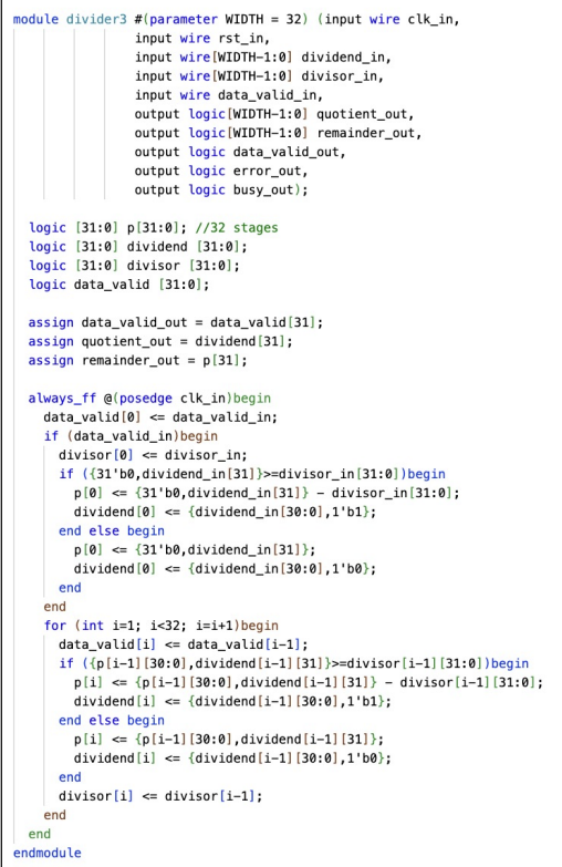
-
Latency stays the same, but throughput increases by a factor of 32!
-
Downside is that resource usage goes way up b/c of so many extra registers
-
can combine the above with multiple subtractions per pipeline stage to get even lower latency divider
-
Which divider you choose depends on your needs (higher throughout? limited resources?)
CORDIC
- What other math things?
- There is a class of iterative algorithms which does can do this sort of stuff
- see here
- This boils down to some very clever shifting and addition
AXI
- For larger blocks, we need a way to send data downstream, but also convey preparedness (ie. signal that the later modules can accept more data) upstream
- For Xilinx IP, the AXI communication protocol is generally used
- Three flavors
- AXI4 (Full): For memory-mapped links. You give an address, them you send a burst of data up to 256 words long
- AXI4 Lite: Memory mapped links, but supports only one data transfer per connections
- Also restricted to 32 bit addresses and data
- AXI4 Stream: High-speed streaming data
- Can do burst transfers of unrestricted size
- No addressing
- Two nodes in AXI protocol: the Main/Controller/Master which directs the Secondary/Peripheral/Slave device
AXI Signals
- ACLK: all modules using AXI must use the same clock
- There can be no combinatorial paths between the inputs and outputs (everything must be registered)
- All signals are sampled on rising edge
- ARSTn: All AXI modules have an active low reset (hence the n part)
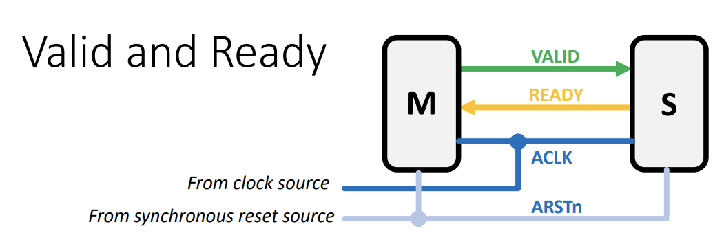
- the creator of data “M” generates a VALID signal
- the destination of data “S” generate a READY signal
- Transfer only occurs when both VALID and READY are high
- The VALID signal of M must not be dependent of the READY signal of s
- S may wait until it detects a VALID signal before it asserts it’s own ready signal
- In other words, READY can depend on VALID, but not the other way around
- This predent dead-lock
- The rest of the wires pass on information
- There can be some additional wires conveying other info (for instance, LAST tells you when you are transmitting the last of the data)
- Can have multiple VALID-READY pairs between two modules (channels)
- For a AXI4 read interface, you need two channels
- One that transfers address info from Master to Slave
- One that transfers response data from Slave to Master
- For AXI4 write interface, need three channels
- Address info from Master to Slave
- Data transfer from Master to Slave
- Response data from Slave to Master
Signed Number
- Signed numbers are represented by two’s complement
- -A = ~A+1 (bit flip, then add one)
- Don’t just flip bits (one’s complement) since you have two representations of zeros
- You can append “signed” to your logic variable, but there are a bunch of gotchas
- If you need to do signed stuff, make every variable signed
- Verilog defaults to unsigned
- So if you want to do signed operations, make sure that both operands are signed
- Based numbers are unsigned, unless there is an explicit “s” modifier
- You can put an “s” in front of constants to make sure they are signed
- Bit-selects are unsigned (ie. a[5] is unsigned)
- Part-select are unsigned (ie. a[4:2])
- concatenations are unsigned
- Sign extension
- The MSB of the number gets extended out into the higher order bits
- Shifts in Verilog do not base themselves off of the type they work with. » is always binary shift
- “»>” tokens result in arithmetic (signed) left and right shifts
- Right shifts maintain the sign by filling in the appropriate sign bit values during shift
- You can force a number be signed by using “$signed” macro, or declare signed type
- Signedness of variable only affect how operators are interpreted
- Some operators are robust to signedness (+,-, bitwise operators, *)
- The interpretation of the operators changes depending on signedness
- If you are doing signed multiplication, make sure, make sure that you sign extend your numbers before you multiply
- It doesn’t just work like the unsigned case
- Also, some operators are sign dependent, which can cause hard to trace bugs
- Also, preappending “-” doesn’t make a number signed
- Remember: -A = 1+ ~A
- The results are not inherently signed
DSP48
- The real world is analog (no shit)
- To transition a signal to digital, you Discretize time and you Quantize the input values
- Discretization
- Errors can arise due to sampling at discrete intervals (high frequency information gets lost)
- You need to sample at a rate which is at least double the highest frequency you want to record (Nyquist’s theorem)
- Higher frequencies can impact the signal, even if they aren’t recorded (called spectral leakage)
- If you don’t meet the Nyquist threshold, then the higher frequencies can appear as a different signal (an “alias”)
- This happens for spatial frequencies too! (hence anti-aliasing filters)
- To avoid aliasing, we need to remove higher frequencies (ie. a low pass filter) prior to sampling
- There are two common types of digital filters
- Infinite impulse response filters (IIR)
- Can model as $y[n] = \alpha y[n-1] + (1-\alpha) *x[n]$ where $y[n]$ is the ouput history and $x[n]$ is the current input
- Increasing $\alpha$ causes the input to have less weight (takes time for input to affact output, which blocks more high frequency events)
- Decreasing $\alpha$ weights the input more (and lets more of high frequency stuff)
- To deal with the fact that $\alpha$ is ostensibly a float, you scale it up by $2^{M}$, and round it off to the nearest integer, then down shift the result after processing
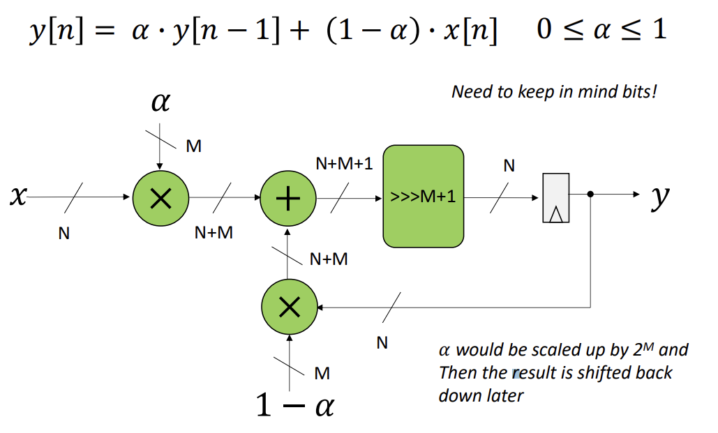
- Can model as $y[n] = \alpha y[n-1] + (1-\alpha) *x[n]$ where $y[n]$ is the ouput history and $x[n]$ is the current input
- Finite Impulse Response (FIR)
- It’s a convolution: $y[n] = b_{0} x[n] + b_{1} x[n-1]+ b_{2} x[n-2]$
- You can have multiple “taps” in an FIR: $y[n] = \Sigma_{k=0}^{N-1} b_{k} x[n-k]$
- Since the $b_k$s can be real numbers between 0 and 1, you can do the $2^{M}$ scaling and shifting trick
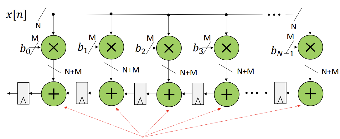
- You can pipelining an FIR to prevent the egregiously long combinational path
- You also need to increase the addition and register sizes every couple of values to avoid loss of precision
- the FIR filter can be implemented interatively via an FSM
- You are given a new input sample
- You use one clock-cycle per multiply-add
- Accumulate the sum, and after N cycles, output a circular buffer (keeps track of past samples)
- You can extend the filter concept to higher dimensions (called kernels)
- Infinite impulse response filters (IIR)
- Quantization
- You want a sufficient bit depth to represent the signal sufficiently
- The higher the bit depth, the smaller quantization error and the more “random” the residuals look like
- There are techniques to make the quantization error look more “random”
- Why? Humans notice patterns better than they notice random patterns
- Common technique is called dithering (common example is Floyd-Steinberg)
- There are techniques to make the quantization error look more “random”
CRCs
- For error corrections, the simplest thing to do is add a parity bit to the end of your message
- This can be easily tricked by a constant number of additional bit flips
- In software, we can implemeent something called a checksum to prevent these type of collisions from happening
- Sum of all of the bits of a blob of data, then take this sum modulo $2^{n}$ to pack the checksum into n bits
- Tack on this checksum to the end of the message
- In hardware, if you are moving across noisy channels, it’s still easy to flip a small number of bits in a message to fool the checksum
- Suppose that you could divide the input by some large number agreed upon by both sender and receiver. The remainder as a function of random bitflips are much less likely to be coincident to the initial method
- One problem: division and modulo of anything other than powers of 2 is extremely slow
Polynomial Arithmetic
- Suppose that we have two numbers $4’b0010$ and $4’b0001$. How do you add them together?
- A strange way of doing this is to transforming the numbers to polynomials. Rewrite the nth least significant bit as the polynomial term $x^{n}$
- so $4’b0010$ becomes $x_{1}$ and $4’b0010$ becomes $x^{0}$
- Setting x=2 yields back the original numbers
- Ignoring that we know that x=2, what is the addition of the two polynomials? That’s just $x^{1}+x^{0}$
- This formalism can be simplified further by taking all of the coefficient mod 2 (so $x^{3}-x^{2}+2x^{1}$ equals $x^{3}+x^{2}$)
- If you play with adding and subtracting numbers like the above, you can see that addition and subtraction acts like an xor
- You can also see that numerical magnitude isn’t really conserved in this system
- As an example: $4’b1000 - 4’b1111 = 4’b0111$ implies $4’b1111 < 4’b1000$, while $4’b1111 - 4’b1000 = 4’b011$ implies $4’b1111 > 4’b1000$
- The only real indication of ordering is the position of the MSB
- $a\geqb$ if and only if a’s most significant 1 appears at an equal or higher index than b’s most significant 1
- Below is an example of doing long division between $8’b1010_1010$ and $5’b10011$
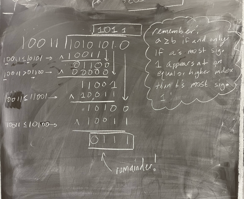
- This division algorithm can be implemented with a Linear Feedback Shift Register, but XORing the input

- You can encode the polynomial of a LFSR as follows (let number of registers be the same as the degree of the polynomial):
- the $x^{k}$ and $x^0$ term correspond to feeding the biggest register back to the smallest (always happens)
- Any intermediate terms of $x^{n}$ have an XOR placed between the n and n+1 register